background image

Summary of Contents for PC-1500

Page 1: ... SHARP SERVICE MANUAL PC 1500 WWW PC 1500 INFO SHARP CORPORATION Do not sale this PDF ...

Page 2: ... General Description 2 Block Diagram 3 3 U l581J 1 0 Port 9 4 Circuit Description 14 5 Servicing 19 6 PC J500 Key Power Supply Circuit 21 PC 1500 Key P W B 22 8 PC 1500 Main P W B 23 9 PC 1500 Main Circuit Diagram 24 IO LCD Segment Back Plate Signal 25 11 Parts List Guide Do not sale this PDF ...

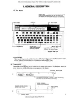
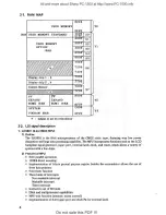
Page 3: ...OWER OFF KEY There are 65 keys in all and their functions differ depending on how whether operation is per formed operated independently or in conjunction with thelSHIFTlkcy 2 Power on off Depression of theIONIkey that is located o n the upper right corner of the keyboard causes the power to tum on 111d the following prompt app au on the llisplay BATTERY INDICATOR _ _____ _J HEl H CHECK L If an op...

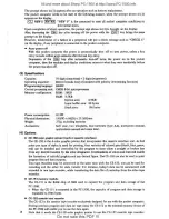
Page 4: ...rea 0 13W 0 9KB 80 bytes 196 bytes I95 W x 86 0 x 25 5 H mm 375g including batteries Soft case two templates four batteries type AA instmction manual applications manual and name label CE 150 color graphic printer built in cassette interface The CE ISO is the 4 color graphic printer that incorporates the cassette interface unit As ball point pen type of stylus is used for printing four varieties o...

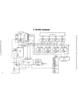
Page 5: ...c Du11l 7 Di9Pl Y Dl flll 7 Q Q ip l C lp4 A0 11I I 0 10 tog Sru f m S rsctm U11e1 RAM RAM KAM TC6 1 0 5KD TC55t O bK8 HlflH 16 i cru LHNOJ L r a I ff _r ISO I ISf m I Vco o AX 11 lt riw _EIAO S 0 RSt 11 jowE H auitr Circui t I 0 PORT LH M10 I c C ime r CJ SZ 1 KHr I i I Pl ll OAC J_ J C n fltl iil ll I NT ikRIBIT DFO arr I cvr Olli rc1 l S 1 1 ADO LS 00 7 Mod Jle Ct mt tor WPir Ill i a 3 Ill er 0...

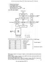
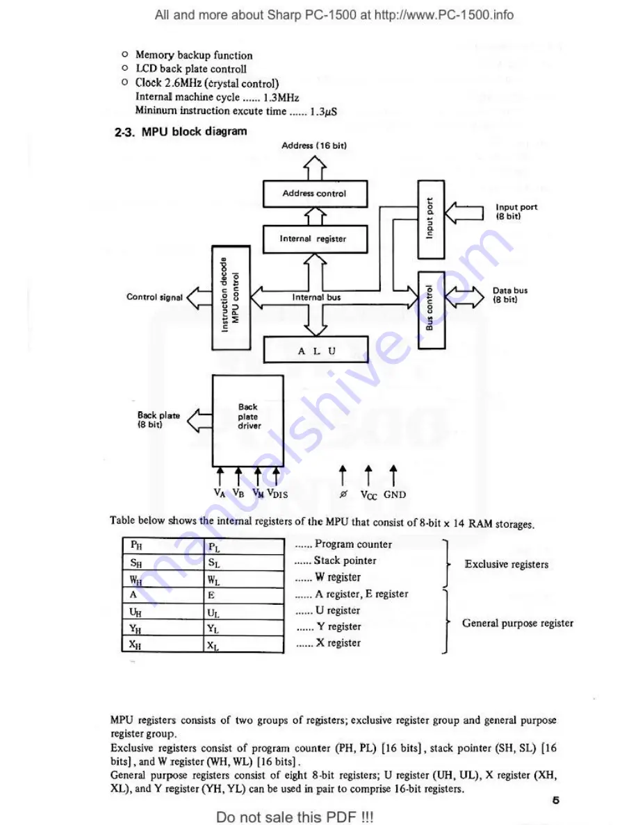
Page 6: ...ability The MPU incorporates functions such as the LCD backplate signal generator input port external latch clock and timer which allows a variety of systems with a few chips 2 Feature of MPU o 8 bit parallel operations o I28KB direct acces ing o Implementation of 6 byte general purpose register besides the accumulator allows the use of three data pointers o 9 bit timer function o Three kinds of i...

Page 7: ...sters of the MPU that consist of8 bit x 14 RAM storages P11 P1 S11 SL Wu WL A E Uu Ur Program counter Stack pointer Wregister A register E register U register iExclusive registers Yn YL Y register General purpose register Xu x X register MPU registers consists of two groups of registers exclusive register group and general purpose register group Exclusive registers consist of program counter PH PL...

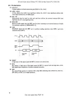
Page 8: ...es for direct accessing to an external memory of which the maximum capacity is 128KB 64KB x 2 5 1 R W Read write signal lhat tlie MPU use to perform reading operation when R W I and writ operation when R W O 0 s ADI x x x L_ MEO I MEI DI IN OUT Data read Data w ite cycle eye le 6 RESET Ahigh input of this signal causes the MPU to return to its initial state 7 BRO Bus request A high state of this s...

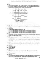
Page 9: ...ction and set to low with the RDP instruction 12 Pip Strobe output is an output during the execution of the ATP instruction normally used for the external latch of the A register contents l13l pos Clock which is in the same pha e as the basic clock inside the chip and it is the basic clock for an entire system It becomes the basic clock of I 3MHz frequency when a 2 6MHz crystal is connected betwee...

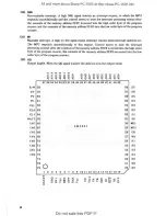
Page 10: ...t the Interrupt pr ssing routine after the contents of the memory address FFF8 is mo ed into the high order byte of the program counter the contents ofthe memory address FFF9 are moved into the low order byte of the program counter 221 OD 011tp11t diS lble When the OD ignal i active the data bus is in the output mode N 0 00 0 t I lO CO CN 0 Q Q Q Q Q Q Q z Q Q Q C Q Q Q Q 0 57 56 55 54 58 52 51 50...

Page 11: ...t ofaccess times can be chosen by programming 5 TI1e following functions are provided for serial control A Serial data transmission Serial data transmission is used in th e format of start bit 8 bit data 2 stop bits Transmission clock is programmable by changing internal and external clocks as well as cha11ging the clock rate 1 1 1 2 1 128 1 256 1 512 1 1024 1 2048 l 4096 of the basic clock B Seri...

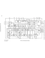
Page 12: ...on control w Sorlll receMr control WAIT control WW U I I II ft l 1 1H f i Chip register i etect control H OAA rt19lator l Brl j l OPB rtQis ter I I OUT PUT control r1 l l i 008 j l register o DATA BUS register control I I I I I L __ _v_________ LJJ ________ ____ l __ __ I _ l _ _J VSS I VSS2 GNJ VCC 4 5 0 SI PA0 7 PB0 7 PC0 7 1 0 PORT controller system block dltgr11m I D0 7 Q WI a WO 3 DMEO Q O 0 ...

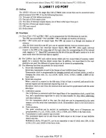
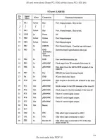
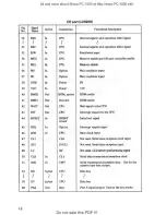
Page 13: ...he timer IC 15 P86 In µPDI990C Data input from the DATA Otrr terminal of the timer IC 16 PB7 In Key BREAK key input interrupt input 17 p In GND PC port latch clock input 18 PCO Out µPD l990C Data output to the DATA IN terminal to the timer IC 19 PC Out µPDl990C Strobe output to the STB tenminal ofthe timer IC 20 PC2 Out µPOl990C Clock output to the LK tenminal of the timer IC 21 PC3 Out µPD1990C T...

Page 14: ... DMEO Out ROM option ROM enable 41 DMEI Out Decoder ROM enable 42 WAIT Out CPU Wait ignal to the CPU 43 INT Out CPU Interrupt request to the CPU 44 RESF T In RESET Initial rest signal circuit 45 IRQ In Option Interrupt request input 46 OS In CPU Basic clock input 47 CLI CLO Not used Serial data reception clock input 48 SDI VCC Not used Serial data reception input 49 LC NC Not used LCD driver synch...

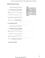
Page 15: ... read from 1 0 port MREQ i __ R1w WAIT vo 1 c b Data wire to 1 0 port Do not sale this PDF NOTE Clock q is furnished to the OS input of the I O port MREQ is an inversion of MREQ of Z 80 and furnished to the MEO of the I O port WAIT is an inversion of WAIT of the I 0 port and furnished to the WAIT input of Z 80 13 ...

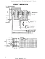
Page 16: ... 2 TC 14r To VO PORT LH5810 To R0ll CS613 128F To MOOul lhi t To Mcdvl lhit tt tou1i Internal logic Truth Table VO A Input ENA BL Sl L1 CT Output Vi 1 8 A c 2 1 Y VJ Y 1 L H H II II II H II F LECT Y2 0 II II II II II II Ii II II II H II II II II Vi II L L L L L I H II II II II c Yi II L L II L L II L II II II II II II L I L L L H H II CIA NA8 f Gtll C l VJ L L H L I II L II L L I L H II II H L H H...

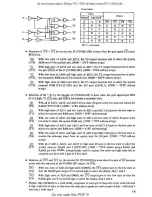
Page 17: ...r RAM area 4800 49FF address setup S2 With low state of AD11 and high state of AD12 and low state ofAD13 S2 goes to the Y2 low state to select the option RAM area 5000 57FF address se tup S3 With high state of ADii and ADl2 and low state of ADl3 S3 goes to the low state to Y3 select the option user RAM area 6000 67FF address setup S6 With low state of AD11 and high state of AD12 and AD13 S6 goes t...

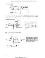
Page 18: ...ircuit R W RAJ II R W CPU 1 AD l O _l l _ W __ F f t t 6 6KO TC5614PX2 pcs 4 ON key double action preventive circuit 16 Vee OAP 202 560KO BFI W l _ 1 5 4 C _ Q I 0 PORT SFI TC50HOOI asr 39PF PS7 P87 This circuit prevents writing if ADIO is in high state during the write mode when R W is low This is to prevent wrong operation when a specific key or I is pushed without performing NEW 0 ENTER after b...

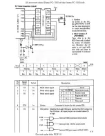
Page 19: ... by 24 hour system IMSBI DIN 9 4 3 2 2 5 2 B Second Minutes Hours Day Week Monti 4 4 I 4 Bits Bits 4 I 4 Bits Bits 4 I 4 Bits Bits 4 4 Bits Bits Bits Signal In out Description name C2 In Mode select signal C2 0 Ci In Mode select signal Cl co Mode Data In out mode co In Mode select signal 0 0 0 Resister hold 0 1 I Registered shirt I 0 2 Time set I 1 3 Time read STB In Strobe Command is latched by t...

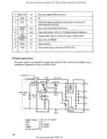
Page 20: ...put ofDATA OUT ENABLE 12 XTAL In Basic clock 32 768KHz 13 XTAL In Same the above 14 YDD In Source power input connected to VGG 4 7V 6 Power supply circuit The power supply is lllCOrporated in 3 Single resin molded IC that consists of the stabilizer circuit temperature compensation circuit and bleeder circuit 18 VBATU HI MIC 18 ri t 14 1 2 SB7_Jc0 __ 2 SB77 9 f o O Vee ADAPTER Jack I SS98 UM 8 X4 2...

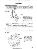
Page 21: ... as a pencial of which the tip is liable to break Also do not use anything with a sharp edge such as a needle up Wait for the prompt l NEW O CHECK to appear on the display then push ICU NEW 0 IENTERI If the prompt NEW O CHECK does not appear try the above entry again Do not use the ALL RESET switch except for the above operation or destruction of the program data and reserve contents will occur 2 ...

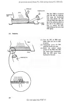
Page 22: ... PWB then apply the tip of the soldering pencil on the side of the soldered sur face to remove the FPC while lifting up the end ofthe FPC lightly I Coat the FPC ad PWB with solder with care not to make it uneven 2 Temporarily secure the FPC using the double tack tape 3 Match the printed circuit pattern of the PWB with FPC and secure them temporarily Slide the FPC about Imm backward in this case Do...

Page 23: ... o r 1 t t r I 13 I 1 lli l t I 0710 fl n9 1 KOj I 4 l t _ _ 1 011rTFlR J I I I I I I I I 1z t L I I WA IMK 120 L _____ J 1 1 Jil O I I I I l_ LTo z J Hi MI C 1 2r 1so s u A LL WM rt 1 so KF Y MA1 WI X l A Do not sale this PDF I I I I I L__ J 3 I 0 1 I 0 1 t 1 I SJS 4 I ls_________ P 1 Vtt vn Ji tit I 21 ...

Page 24: ...All and more about Sharp PC 1500 at http www PC 1500 info Do not sale this PDF ...

Page 25: ...Pc 15 lgn tl 2 tt2 tJ fw 1 i _pjl into PC 1500KEY PWB From the February I 982 Production ____________ _ ___________________ _______ I Do not sale tnis PDF T ...

Page 26: ...All and more about Sharp PC 1500 at http www PC 1500 info Production ____________ o not sale ihis F Dr 1___ ...

Page 27: ...PC NJOOM B rp iabJJUN Bar t CQa rj 1 500 info PC 1500 MAIN PWB From the February I 982 Production I L L__r Do not sale this PDF ...

Page 28: ...All and more about Sharp PC 1500 at http www PC 1500 info 2 Production _J Do not sale this PDF ...

Page 29: ...pc_15oo MA00a19 W 8abff9 f W a ttpytwww PC 1500 info PC 1500 MAIN P W B From the July 1982 Production 0 Do not sale this PDF ...

Page 30: ...All and more about Sharp PC 1500 at http www PC 1500 info Do not sale this PDF ...

Page 31: ...All and more about Sharp PC 1500 at http www PC 1500 info 10 LCD SEGMENT BACK PLATE SIGNAL l l V I I 5 Do not sale this PDF u1 uuu t u 1 1 11 1 1 11u u u lhl I I I I I I I I I I ...

Page 32: ...J J ut n11u1 All and more about Sharp PC 1500 at http www PC 1500 info If iJ 3 0 l l l J I r r 1 r t 8 cl I U I I I I I I I Do not sale this PDF l o I 25 ...

Page 33: ...JKNBZ 5 15CC l 2 Key top 1so 20PCS N c A F 11 14 JKNBZ 493CC03 Key top 1set 30PCS N c A E 12 P GUMM 389CCZZ Key rubbor N c A L 13 DUNTK6381CCZZ Key PWB unit N E c A 14 LX BZI060CCZZ Screw N c A A 15 Q JAKCI003CCZZ Jack sockdet c A D 16 PZETL l427CCZZ Insulato r N c A A 17 LANGT l 439CCZZ An 1lc 8 N c A c 18 QPWBM2027CCZZ FPC N c A _ 19 LANGTl438CCZZ Angle A N c A 0 20 XNE5D20 16000 Nu1 c A A 21 QC...

Page 34: ...NE I 022CCZZ Program libraty English N 0 A z T MANGl023CCZZ Pr Jram library Germany N 0 UBAGCl290CCZZ Soft case N 0 A R VHDDSl566L l I D iode 1 srnssL1 B A D VHO I SS98 I Diode N 8 A 0 V HHl 54KD 5 I Thermistor 150Kohm B A c j_ VH i EHM7 I SL70N I C Power regurator N 8 A T _ _VH i HM6 11 6 C I1 C HM61 16 N B B H I VHiLH580 1 I l S I LH5801 N 8 8 K VH i LH58 I I I L S I LH5811 or 5810 N 8 A z VHiSC...

Page 35: ...All and ww PC 1500 info more about SharP PC 1500 at http w D o not sale th IS PDF Ill ...

Page 36: ... 12 13 9 All and more about Sharp PC 1500 at http www PC 1500 info Do not sale this PDF ...

Page 37: ...I 1 1 ti ii E Ll Ir j I it r I I I r l I i r _ onot sale this PDF I I 1 i I I I I r c 11 t I ...

Reviews:

Related manuals for PC-1500