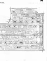
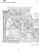
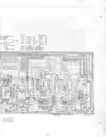
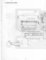
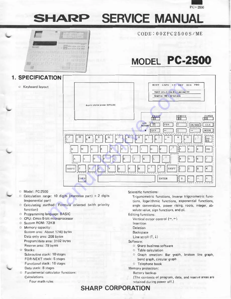
Sharp pc-2500, Service Manual
The Sharp PC-2500 Service Manual is a comprehensive user guide for this classic handheld computer. Providing detailed instructions and troubleshooting tips, this manual is available for free download at 88.208.23.73:8080. Equip yourself with this essential resource to maximize the functionalities of your PC-2500.
Share
Download
Reviews:
No comments
Related manuals for pc-2500
Numpad Break
Brand: R-Go Pages: 14
Compact
Brand: R-Go Pages: 11

2100
Brand: Hama Pages: 10
Nimble
Brand: Hama Pages: 10

98091
Brand: GE Pages: 9
V3
Brand: WASD Pages: 4
Wireless Keyboard
Brand: Palm Pages: 20
FZ-VKBQ11 Series
Brand: Panasonic Pages: 4
SXKC600 - ELECTRONIC KEYBOARD
Brand: Panasonic Pages: 48
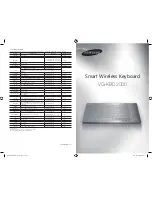
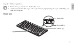
VG-KBD2000
Brand: Samsung Pages: 10
EJ-BT230
Brand: Samsung Pages: 11
AK-120
Brand: Hama Pages: 2
MiniPad
Brand: B-Speech Pages: 12
FS900
Brand: Kawai Pages: 48
H SERIES
Brand: CAME Pages: 2
K5
Brand: Xtrfy Pages: 15
smart
Brand: Magicforce Pages: 2
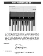
MP-1
Brand: Fatar Pages: 3


