


28
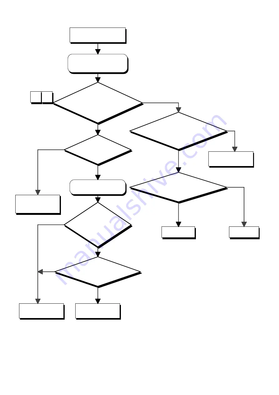
Composite Sync. Signal
Display Check.
Input a composite sync.
signal.
(MAC II type: 30.24MHz)
Check IC206-pin6.
Is clock pulse of
approx.30.24MHz inputted to
IC100-pin116
(VCOIN)?
Is IC100-pin108 at a
low level?
Disconnect the signal cable
from J2.
Is proper level video signal at
signal cable-pin1,2,3?
Input circuit failure.
Is Hsync inputted to IC100-
pin109?
Is Vsync inputted to IC100-
pin110?
Is clock pulse of
approx.25.00MHz inputted to
IC100-pin19?
IC100 failure.
OSC1 failure.
Failure of analog
threshold level setting
circuit.
Signal cable failure.
Is signal cable-
pin9(MAC) shorted
to GND?
Is signal cable-pin10
(A/D) GND?
Failure of signal cable
or input circuit.
No
No
No
No
No
No
Yes
Yes
Yes
Yes
Yes
Yes
7
8
Summary of Contents for QD-101MM
Page 39: ...38 6 CIRCUIT DIAGRAM PWB Fig 27 CIRCUIT DIAGRAM MAIN CIRCUIT No 1 ...
Page 40: ...39 Fig 27 CIRCUIT DIAGRAM MAIN CIRCUIT No 1 ...
Page 41: ...40 Fig 28 CIRCUIT DIAGRAM MAIN CIRCUIT No 2 ...
Page 42: ...41 Fig 28 CIRCUIT DIAGRAM MAIN CIRCUIT No 2 ...
Page 43: ...42 Fig 29 CIRCUIT DIAGRAM MAIN CIRCUIT No 3 ...
Page 44: ...43 Fig 29 CIRCUIT DIAGRAM MAIN CIRCUIT No 3 ...
Page 45: ...44 Fig 30 CIRCUIT DIAGRAM MAIN CIRCUIT No 4 ...
Page 46: ...45 Fig 30 CIRCUIT DIAGRAM MAIN CIRCUIT No 4 ...
Page 47: ...46 Fig 31 CIRCUIT DIAGRAM POWER CIRCUIT ...
Page 48: ...47 Fig 31 CIRCUIT DIAGRAM POWER CIRCUIT ...
Page 49: ...48 Fig 32 CIRCUIT DIAGRAM VIDEO CIRCUIT ...
Page 50: ...49 Fig 32 CIRCUIT DIAGRAM VIDEO CIRCUIT ...
Page 51: ...50 Fig 33 CIRCUIT DIAGRAM AUDIO CIRCUIT ...
Page 52: ...51 Fig 33 CIRCUIT DIAGRAM AUDIO CIRCUIT ...
Page 53: ...52 Fig 34 PWB PATTERN MAIN PWB FRONT SIDE ...
Page 54: ...53 Fig 34 PWB PATTERN MAIN PWB REAR SIDE ...
Page 66: ...PRINTED IN GERMANY ...


