TM150
ADJUSTMENTS, PERFORMANCE CHECK, AND FIRMWARE UPGRADE
2 – 36
CONFIDENTIAL
DRAFT
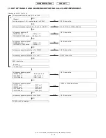
11. OUT OF RANGE AND INCOMING/OUTGOING CALLS ARE IMPOSSIBLE.
[Checkpoint s in RF Test Tool ]
Is transmission possible using RF Test Tool?
Is voltage (applox. 2.9 V) supplied to pin 6 of IC804?
IC804 is defective.
Is IQ signal supplied to pins 23, 24, 25, and 26 of IC801?
IC103, IC106, or PWB is defective.
Is frequency signal sent?
GSM 900 bands ....................... IC801 pin 17
DCS1800/PCS1900 bands ...... IC801 pin 19
IC801 is defective.
Is frequency signal supplied?
GSM900 bands ....................... IC803 pin 15
DCS1800/PCS1900 bands ..... IC803 pin 13
IC802 is defective.
Is frequency signal supplied to pin 1 of FL905?
IC803 is defective.
Is frequency signal supplied to pin 1 of J801?
FL905 is defective.
J801 is defective.
[Receiver]
–70 dBm input.
Is frequency signal supplied?
GSM900 bands
.............
............. .
IC801 pins 9, 10
DCS1800 band ............................ IC801 pins 6, 7
PCS1900 band ............................ IC801 pins 3, 4
IC801 is defective.
Is frequency signal supplied?
GSM850 band ................................ FL901 pin 1
GSM900 band ................................ FL902 pin 4
DCS1800 band ............................... FL902 pin 1
PCS1900 band ............................... FL903 pin 1
FL902, or FL903 is defective.
Is frequency signal supplied to pin 9 of IC803
IC803 is defective.
FL905 or J801 is defective.
YES
NO
[Sender]
NO
YES
NO
YES
NO
YES
NO
YES
NO
YES
NO
YES
YES
NO
YES
NO
YES
NO
Summary of Contents for TM150
Page 61: ...TM150 CIRCUIT DIAGRAM AND PWB LAYOUT 5 13 CONFIDENTIAL DRAFT MAIN PWB_FRONT ...
Page 62: ...TM150 CIRCUIT DIAGRAM AND PWB LAYOUT 5 14 CONFIDENTIAL DRAFT MAIN PWB_REAR ...
Page 63: ...TM150 CIRCUIT DIAGRAM AND PWB LAYOUT 5 15 CONFIDENTIAL DRAFT LCD PWB_FRONT ...
Page 64: ...TM150 CIRCUIT DIAGRAM AND PWB LAYOUT 5 16 CONFIDENTIAL DRAFT LCD PWB_REAR ...


