background image

UP-3301US

SERVICE PRECAUTION

– 18 –

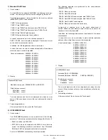
5. Requirements for soldering circuit parts

To solder the following parts manually, follow the conditions described
below.

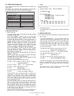
6. Note for handling of Touch panel

•  The transparency of the touch panel is vitally important. Do not place

finger prints or moisture on the surface. When handling, use clean
gloves and masks.

• For handling, do not hold the transparent area, and do not hold the

heat seal connector section to assure reliability. 

•  Do not overlay touch panels. The edge may damage the surface. 

•  Do not put a heavy object on the touch panel.

•  Do not apply strong shocks, and do not drop.

•  When attaching the protection film, carefully check that no dirt exists. 

•  To clean dirt on the surface, use a dry, soft cloth or a cloth immersed

in ethyl alcohol.

• Check that the housing does not induce any stress to the touch

panel. 

•  Be careful not to touch the touch panel with tools. 

• The heat seal section is easily disconnected. Be careful not to apply

any stress to the heat seal section when installing. 

• The touch panel is provided with an air groove to make the external

and the internal air pressure equal to each other. If water or oil is put
around the air groove, it may penetrate inside. Be careful and keep
the air groove away from water and oil. 

• Input is performed with fingers. Do not use hard objects to input

entries.

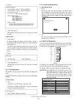
7. Note for handling the LCD assembly

•  The LCD elements are made of glass. BE careful not to expose them

to a strong mechanical shock. Use extreme care not to break them.

• If the LCD element is broken and the liquid is seeps, do not lick it. If

the liquid comes in contact with your skin or clothes, immediately
clean with soap. 

•  Use the unit under the rated conditions to prevent against damage.

•  Be careful not to drop water or other liquids on the display surface.

• The reflection plate and the polarizing plate can be easily scratched.

Be careful not to touch them with any hard object such as glass or
tweezers. Never hit, push, or rub the surface with hard objects.

• When installing the unit, be careful not to apply stress to the LCD

module. If excessive stress is applied an abnormal display or uneven
color may result. 

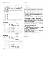
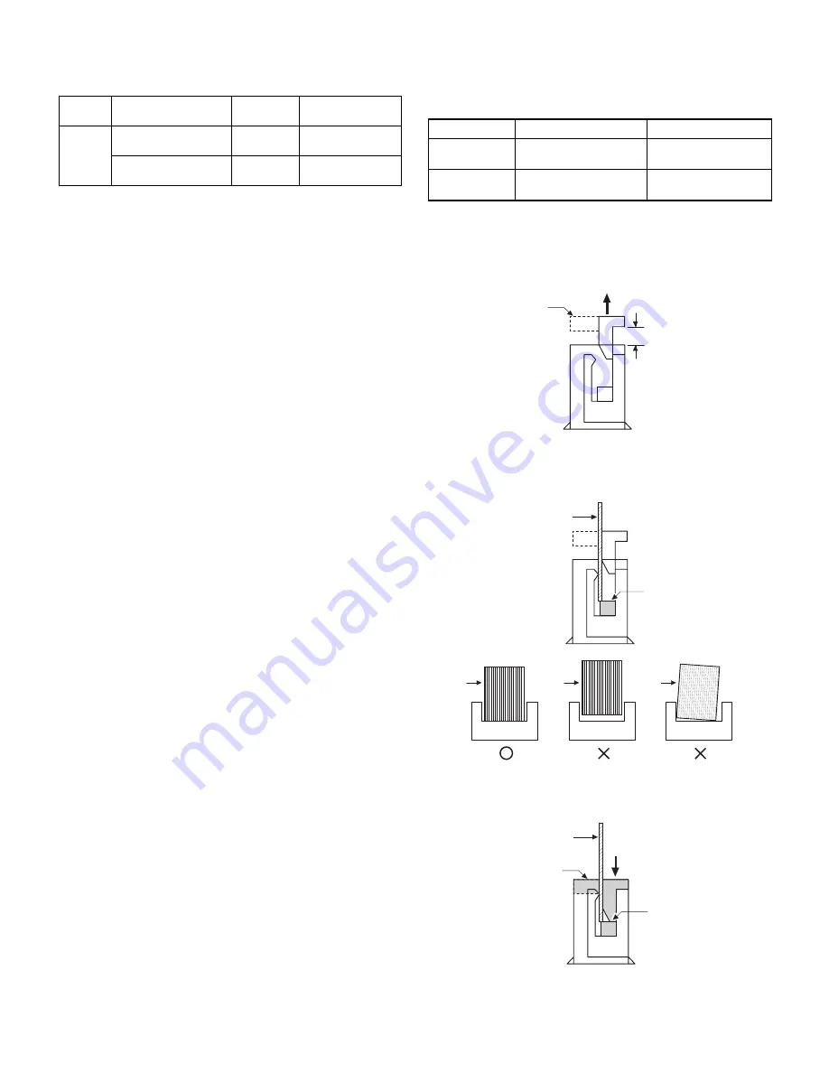
8. Cautions on handling connectors

When connecting or disconnecting the following connectors, follow the

procedures below.

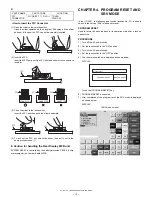
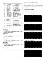
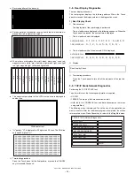
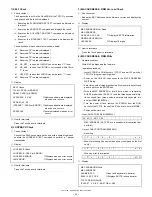
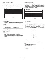
1)

 • How to Connect or Disconnect the FFC Connector

(1) Open the slider to the unlock position

The slider will open only up to a fixed height (about 1.2mm). If you

used force to pull up the slider further, it may be damaged.

(2) Insert the FFC

Insert the FFC firmly untill the FFC hits the bottom of the connec-

tor’s insulator.

(3) Close the slider to the lock position

Insert the FFC and then push the slider downward.

PARTS 

NAME

PARTS CODE

LOCATION

CONDITIONS FOR 

SOLDERING

Ceramic 
oscillator

RCRMZ7002RCZZ

MAIN PWB: 
X1 (8M)

270°/3sec.

RCRMZ7004RCZZ

MAIN PWB: 
X2 (7.37M)

270°/3sec.

PARTS NAME

PARTS CODE

LOCATION

FFC 
CONNECTOR

QCNCW7207RC4J

MAIN PWB: CN6
TOUCH PWB: CN5

FFC 
CONNECTOR

QCNCW7183BH2F

MAIN PWB: CN1

Slider

1.2mm

UNLOCK

FFC

FFC

CONNECTOR

FFC

CONNECTOR

FFC

CONNECTOR

FFC

Slider

LOCK

Summary of Contents for UP-3301

Page 1: ...e used for after sales service only The contents are subject to change without notice SERVICE MANUAL UP3301USME POS TERMINAL MODEL UP 3301 For U A version CHAPTER 1 SPECIFICATIONS 1 CHAPTER 2 OPTIONS 7 CHAPTER 3 SERVICE PRECAUTION 9 CHAPTER 4 PROGRAM RESET AND SRV MODE 16 CHAPTER 5 MASTER RESET ALL MEMORY CLEAR 17 CHAPTER 6 DIAGNOSTICS SPECIFICATIONS 20 CHAPTER 7 CIRCUIT DESCRIPTION 31 CHAPTER 8 C...

Page 2: ... BATTERY TERMINALS KEEP THE BATTERY AWAY FROM FIRE WHEN DISPOSING THE BATTERY FOLLOW THE LOCAL RULES AND REGULATIONS BATTERY DISPOSAL THIS PRODUCT CONTAINS NICKEL METAL HYDRIDE BATTERY THIS BATTERY MUST BE DISPOSED OF PROPERLY REMOVE THE BATTERY FROM THE PRODUCT AND CONTACT FEDERAL OR STATE ENVIRONMENTAL AGENCIES FOR INFORMATION ON RECYCLING AND DISPOSAL OPTIONS ...

Page 3: ...he display can be tilted to the best viewing angle by sliding the rear stand External dimensions 11 6 W x 16 3 D x 12 6 H in 295 W x 414 5 D x 320 H mm Weight 14 6 lbs 6 6 kg Power source 120V AC m 10 60 Hz Power consumption Stand by 27W Operating 51W max Working temperatures 32 to 104 F 0 to 40 C Operator display touch panel Top cabinet Money checking space IPL cover Brightness control Contrast c...

Page 4: ...lay Window Status indication Mode caption Time Touch panel keyboard Display Window In the PGM mode programmable items are listed Server code Mode caption Time Server name Double size character mode indicator W Appears when the d ouble size character mode is selected during text programming Double size character mode indicator W Appears when the d ouble size character mode is selected during text p...

Page 5: ...2 000003 000004 000005 MODE CLEAR P UP P DOWN HOME CANCEL MORE VOID RFND MORE D THRU PAYMEN QTY DISC MISC G CHK MGR MENU01 MENU02 MENU03 MENU04 MENU05 L1 L2 L3 SUB 000026 000027 000028 000029 000030 000021 000022 000023 000024 000025 000016 000017 000018 000019 000020 MODE CLEAR P UP P DOWN HOME CANCEL MORE VOID RFND MORE D THRU PAYMEN QTY DISC MISC G CHK MGR MENU01 MENU02 MENU03 MENU04 MENU05 L1 ...

Page 6: ...ries MODE CLEAR P UP P DOWN HOME CANCEL 00 2 3 5 6 8 9 7 4 1 0 VOID SUB RFND TAX1SF TAX2SF TAX SRV RCP SW RCPT WASTE REPEAT RP SND MGR ENTER RLU SB D THRU PAYMEN MODE CLEAR P UP P DOWN HOME CANCEL 00 2 3 5 6 8 9 7 4 1 0 N C PBAL MFUNC VOID SUB RFND PAYMEN ENTER CVCNT SRV MGR QTY DISC MISC MGR MODE CLEAR P UP P DOWN HOME CANCEL 00 2 3 5 6 8 9 7 4 1 0 RETURN VOID RFND ST VD RCP SW RCPT BILL EMPL E S...

Page 7: ... past item or used for the cursor void function ST VD Used to void an entire transaction subtotal void RFND Used to enter the refund item RETURN Used to enter the returned item 1 thru 9 Used to enter the percent calculation percent 1 thru 9 1 thru 9 Used to execute the discount entry discount 1 thru 9 TAX Used to enter the manual tax CV CNT Used to enter the cover count AUTO to AUTO7 Used to enter...

Page 8: ...eak in out operations QTY Used to go to the function menu 1 keyboard q ty entry DISC Used to go to the function menu 2 keyboard discount percentage entry MISC Used to go to the function menu 3 keyboard the miscellaneous function keyboard G CHK Used to go to the function menu 4 keyboard guest check entry MGR Used to go to the function menu 5 keyboard Manager Server Employee entry FUNC 6 Used to go ...

Page 9: ...M board 5 On line function RS232 I F board ER A7RS2 2 port RS232 I F 6 OTHER MCR Magnetic Card Reader UP E12MR2 for ISO 1 2 stripe card Satelite HUB PC Local purchased RS 232 Communication PC Local purchased Scale Local purchased CAT Local purchased RS 232 R J Printer Option ER 01PU MCR Option UP E12MR2 Poll Display Option UP P16DP RS 232 Board Option ER A7RS2 Max 6ports Master terminal LAN Remote...

Page 10: ...executing the diagnostics for the UP E12MR2 External view No NAME PARTS CODE PRICE DESCRIPTION 1 MCR test card UKOG 6718RCZZ BE for UP E12MR2 2 RS232 loop back connector UKOG 6705RCZZ BC for RS232 connector 3 Expansion PWB CKOG 6724BHZZ BX for ER A7RS2 Test pins Used to check the bus signals Bus connector Used to check the bus signals Connected to the UP 3301 Mother PWB UP 3301 bus connector ER A7...

Page 11: ...a are those of the initial coordinates Refer to the table below The point from where the finger leaves the touch panel is defined as the correction point input position OFF position The data on the nearest correction point is checked and if almost appropriate regarding data of the initial coordinates within 100 dots and 5mm in size the command correction data set is issued to the controller When t...

Page 12: ...when replacing the main PWB unit 2 IPL procedure There are two ways of IPL procedures IPL from EPROM via ER A7RS2 IPL from PC via the POSUTIL EXE PC utility The detailed descriptions on the above procedures are given below 3 IPL from P ROM via ER A7RS2 1 Install the two master ROMs to the IC socket IC12 IC13 on the ER A7RS2 Master ROM 1 VHI27801RXXXX Master ROM 2 VHI27801RXXXX 2 IPL switch on the ...

Page 13: ...ng 3 PROCEDURE 3 1 POS UTILITY POSUTILITYTOOL EXE IPL of UP 3301 Program Object 02FD EXE All RAM Data Upload Download PC software tool instead of the current ER 02FD PC D SUB 9pin D SUB 9pin cable D sub 9pin CD RD SD ER GND DR RS CS CI 1 2 3 4 5 6 7 8 9 1 2 3 4 5 6 7 8 9 RD SD GND PC UP 3301 D sub 9pin No Procedure on P C side No Procedure on UP 3301 side 1 Install the POSUTILITYTOOL EXE on the P ...

Page 14: ...D button Program data is sent to the UP 3301 automatically 9 Program data is received from the P C automatically The UP 3301 displays 10 When data sending is completed the initial Window is shown after Complete window 10 The UP 3301 displays Completed 11 Turn OFF the power 12 Select Normal Mode Set the IPL switch to OFF 13 Execute the Service Reset on UP 3301 No Procedure on P C side No Procedure ...

Page 15: ...the P C Please close all other applications while using this utility 5 Set the Communication method by pushing the Setting Button Push the OK Button 6 Push the POS 3 PC Button And Select the Receiving File 7 Communication starts 7 Push CASH key The UP 3301 displays 8 The UpLoad is completed The initial Window is shown Push the Exit Button 8 The UpLoad is completed The SETTING menu is shown 9 ALL R...

Page 16: ... The LOGO STAMP data for the UP T80BP is set Black and white BMP PCX data is used and the image size is up to 576 x 240 dots 3 Program rewrite IPL The UP T80BP program is updated S type files are used for ROM data According to the contents of the file UTL33 EXE automatically selects the appropriate protocol from the three types described above 1 11 Execute the 02FD EXE on the P C Please close all ...

Page 17: ...1_2 ROM are file name of S type ROM object 8 Program data is sent to UP 3301 automatically 8 Program data is received from P C automatically The UP 3301 displays 9 UTL33 EXE is completed P C shows Completed 9 The UP 3301 displays Completed 10 Turn OFF the power 11 Select Normal Mode Set the IPL switch to OFF 12 Execute the Service Reset on UP 3301 IPL SW ON IPL from IR Connected IRDA 115200 21 22 ...

Page 18: ...GO BMP LOGO BMP is a file name of Bit Map image 9 Program data is sent to UP 3301 automatically 9 Program data is received from P C automatically 10 UTL33 EXE is completed P C shows Completed 10 UP 3301 shows Completed And UP T80BP prints out the LOGO image 11 Touch OK button 12 Touch EXIT button 13 Turn OFF the power of UP 3301 14 Execute Master Reset on UP T80BP No Procedure on P C side No Proce...

Page 19: ...pplication program which is in its own flash ROM The ERROR Lamp is blinking and the On Line Lamp is turned off 6 UP T80BP waits the application program data The ERROR Lamp is turned off and the On Line Lamp is turned on 7 Enter UP T80BP Utility mode Select 6 UP T80BP Utility in SRV mode 8 Starting of UP T80BP Utility mode UP 3301 shows 9 Connect P C and UP 3301 via RS232 CH2 10 Execute UTL33 EXE o...

Page 20: ...ot to expose them to a strong mechanical shock Use extreme care not to break them If the LCD element is broken and the liquid is seeps do not lick it If the liquid comes in contact with your skin or clothes immediately clean with soap Use the unit under the rated conditions to prevent against damage Be careful not to drop water or other liquids on the display surface The reflection plate and the p...

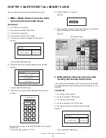
Page 21: ... microcomputer on the rear display PWB CHAPTER 4 PROGRAM RESET AND SRV MODE In the UP 3301 the following reset switch location No S1 is used to switch to the service SRV mode and to reset PROGRAM RESET Used to return the machine back to its operation state after a lock up has occured PROCEDURE 1 Turn off the AC power switch 2 Set the reset switch to the ON position 3 Turn on the AC power switch 4 ...

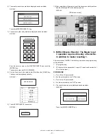
Page 22: ... key The secret number for MRS 1 11111111 8 MASTER RESET 1 is executed DISPLAY 9 After completion of the master reset the buzzer sounds three times and the following SRV mode display is shown DISPLAY SRV mode screen 2 MRS 2 Master Reset 2 Clear the entire memory and resumes initial values The keyboard must be entered by hand This reset is used if an applica tion needs different keyboard layout oth...

Page 23: ...e screen 3 MRS 3 Master Reset 3 The Master reset 3 operation requires the entry of Serial No in addition to master resetting 1 After completion of a MRS3 the following operations and programming will be inhibited 1 GT programming 2 GT resets with the transaction Z report Z report can be made but GT will not be reset PROCEDURE 1 Turn off the AC power switch 2 Set the reset switch to the ON position...

Page 24: ...yed as shown below DISPLAY Enter the serial No of the POS and touch the ENTER key 9 Set the fixed keys in the table below Start from the HOME key The keys are displayed sequentially DISPLAY 10 MASTER RESET 3 is executed DISPLAY 11 After the completion of the master reset the buzzer sounds three times and the following SRV mode display is shown DISPLAY SRV mode screen MASTER RESET Please select MAS...

Page 25: ...M is replaced 5 Perform CALIBRATION when either the touch panel or the EE ROM was replaced 6 Select the MASTER RESET from the menu and execute it 2 Program reset service reset procedure 1 Turn off the AC power switch 2 Set the reset switch to the RESET position 3 Turn on the AC power switch 4 Set the reset switch to the normal position Do not press the touch panel 5 Select PROGRAM RESET from the m...

Page 26: ...S1 PASS6 an error display is made If there is no error at all the check is normally terminated In addition the following address check is performed in the above test sequence In case of an error an error display is made and the read write address of the where the error occurred is repeated 2 Display The error address and the bit are displayed only when the error occurs If the error does not occur ...

Page 27: ...it possible to control the program version by the chip the program version stored in the blocks 21H 31H 41H and 51H are displayed If the beginning of each ROM version stored in the blocks 21H 31H 41H and 51H is not 27801R or sample it is regarded that the area does not have any program stored and thus no program version is displayed In addition the 0 PAGE Block where IPL is stored shows the pro gr...

Page 28: ...ound is heard and the rectangle turns black when each posi tion is touched 2 End The test is over when the four corners have been touched To exit please press the touch panel 3 6 RS232 I F Diagnostics The main PWB and the optional PWB RS232 interface of ER A7RS2 are checked Attach the 9 pin D Sub loop back connector UKOG 6717RCZZ The wiring diagram is shown below Fig 6 1 Fig 6 1 The following menu...

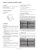
Page 29: ... when each signal is active or if an inter ruption is made when each signal is not active an error display is made The above check is repeated in four cycles Data transfer check The loop back data 256 bytes of 00H 0FFH are used for the data transfer check The baud rate is set to 38400BPS Timer check RS232 on board timer Before performing the check set the timer to TCVDT start and 5ms Then perform ...

Page 30: ...splay returns to the menu screen 1 Liquid Crystal Display Check 1 Check content The test patterns are displayed in the following sequence When the Touch panel is pressed the next pattern is displayed i Black and white pattern at 1 dot pitch ii Reversed pattern of the above i iii Vertical stripe pattern at 1 dot pitch iv Reversed pattern of the above iii v Horizontal stripe pattern at 1 dot pitch E...

Page 31: ...ouch panel to turn off all the elements of the rear dis play 3 9 TCP IP Stack Network Diagnostics Performing the TCP IP STACK test To perform this test the following configuration is required UP 3301 10BASE T cable only for data transmission test HUB only for LOOPBACK test and data transmission test when using satellites The following menu is displayed Touch the key of the operation you want to ex...

Page 32: ...de 08 00 1F and the three hexadecimal dig its converted from three numbers entered with keyboard into dual port RAM 800000H Turn the power off and remove the EPROM from the ROM socket of the TCP IP then set the IPL switch to normal MODE Power on the main unit Input DUAL PORT RAM 80000H MAC ADDRESS XX YY ZZ are in hexadecimal converted from decimal Output DUAL PORT RAM 800800H Rewriting When termin...

Page 33: ...key The following screen appears The numeric key panel to enter numeric characters is displayed in the lower part of the screen Press the terminal No 2 digits number among 1 16 of the sat ellite machine to be connected to the test machine The numeric key panel to enter numeric characters is displayed in the lower part of the screen When checking with two or more satellite machines connected repeat...

Page 34: ... Terminating procedure Press the Touch panel to terminate the check Data Trans MA INPUT MA T NO XX INPUT SA T NO XX XX XX XX XX XX XX XX XX XX XX XX XX or XXXX DATA SEQ NO 0000 TCP IP ERROR XX Displays ERROR CODE 01 Improper command except when transmission 02 No data received 03 Received data present Received data remained 04 Remote machine not ready when sending NTDY is sent back because the rem...

Page 35: ...pears Press the name of the test you want to perform to execute its Diag program When the Diag program is termi nated the screen returns to the Printer Diagnostics menu Pressing the CANCEL key returns to screen to the Diag Menu 1 Loop Back Check 1 Check A LOOPBACK test on the built in printer UP T80BP interface logic channel 7 of RS232 is performed and the result is displayed The test itself is th...

Page 36: ...8 Customer display MCR SRAM 2MB OPC2 EXT SLOT 80pin x 2 RAMCN 72pin CKDC9 VCC 24V 12V LCD 640 x 480 dots DRIVER DRIVER DRIVER RECEIVER VGA CONTROLLER MN89303A BRIGHTNESS CONTROL INVERTER CONTRAST ADJUSTMENT POWER SUPPLY VRAM DRAM 512K UPE10IN Compatible FLASH RAM 4MB NOR PRINTER UP T80BP Clerk SW TCP IP TOUCH CONTROLLER x 2 ...

Page 37: ...XD1 SCK2 IRQ3 SCK1 IRQ2 IRQ1 IRQ0 VCC AVCC P73 P72 112 111 110 109 108 107 106 105 104 103 102 101 100 99 98 97 96 95 94 93 92 91 90 89 88 87 86 85 P41 P42 P43 P44 P45 P46 P47 VSS P50 P51 P52 P53 P54 P56 P57 P60 P61 P62 P63 P64 P65 P66 P67 VSS AVSS P70 P71 57 58 59 60 61 62 63 64 65 66 67 68 69 70 71 72 73 74 75 76 77 78 78 80 81 82 83 84 A8 A9 A10 A11 A12 A13 A14 A15 VSS A16 A17 A18 A19 A20 A21 A...

Page 38: ...FSH EXTAL XTAL E P17 P16 P15 P14 P13 P12 P11 P10 D15 D14 D13 D12 D11 D10 D9 D8 P57 P56 P55 P54 P53 P52 P51 P50 P67 P66 P65 P64 P63 P62 P61 P60 P73 P72 P71 P70 TXD2 RXD2 TXD1 RXD1 SCK2 IRQ3 SCK1 IRQ2 IRQ1 IRQ0 H8 500 CPU DTC Serial communication interface x 2ch 8bit timer 16bit free running timer x 2ch Refresh controller Wait state controller A D converter Interruption controller Clock oscillator W...

Page 39: ...T In MCR interrupt signal 61 P45 GND In GND 62 P46 SHEN In CKDC interface shift enable signal 63 P47 GND In GND 64 VSS GND In GND 65 P50 ER Out DTR signal for RS 232 CH8 66 P51 DR In DSR signal for RS 232 CH8 67 P52 CS In CTS signal for RS 232 CH8 68 P53 CD In DCD signal for RS 232 CH8 69 P54 RR Out RR signal for RS 232 CH8 70 P55 RS Out RTS signal for RS 232 CH8 71 P56 CI In RI signal for RS 232 ...

Page 40: ...132 GND 131 DT1 130 DT2 129 DT3 128 DT4 127 RJTMG 126 TPCKI 125 TPTXD 124 RAS2 123 ROS2Z 122 ROS1Z 121 OPTCSZ 41 ID3 42 GND 43 ID4 44 ID5 45 ID6 46 ID7 47 SSPRQZ 48 RESETZ 49 INT2Z 50 INT3Z 51 RXDI 52 TXDI 53 SCKI 54 IRQ0Z 55 A0 56 A1 57 A2 58 A3 59 A4 60 A5 61 GND 62 VDD 63 A6 64 A7 65 A8 66 A9 67 A10 68 A11 69 A12 70 A13 71 A14 72 A15 73 A16 74 A17 75 A18 76 A19 77 A20 78 A21 79 A22 80 LCDCZ 120...

Page 41: ...Z CLS1 RCP1 RDD1 CLS2 RCP2 RDD2 TPTRDYZ TPTXD TPRXD TPCKI TPRDY TPRRDYZ SSPRQZ TXDI SCKI RXDI SCK1 STH2 HTS2 SCK2 STH2 HTS1 INT1Z INT2Z INT3Z EXINT0Z EXINT1Z EXINT2Z INT4Z TESTZ TEST0 TEST1 TEST2 MD0 MD1 IRQ02 EXINT3Z DECODE BUFFER READ WRITE CONTROL WAIT CONTROL MCR I F USART X2 TOUCH PANEL I F USART SSP COMPARISON REGISTER BAR SERIAL CHANNEL SELECT for CKDC INT CONTROL TEST LOGIC M P C A 8 A23 A...

Page 42: ... BUS 46 ID7 IO DATA BUS 47 SSPRQZ O SSP REQUEST FOR CPU 48 RESETZ ICS MPCA RESET 49 INT2Z ICU INTERRUPT INPUT TPRRDY 50 INT3Z ICU INTERRUPT INPUT TPTRDY 51 RXDI O SERIAL OUT FOR CPU 52 TXDI IS SERIAL IN FROM CPU 53 SCKI IU SERIAL CLOCK FROM CPU 54 IRQ0Z O INTERRUPT SIGNAL FOR CPU 55 A0 I ADDRESS BUS 56 A1 I ADDRESS BUS 57 A2 I ADDRESS BUS 58 A3 I ADDRESS BUS 59 A4 I ADDRESS BUS 60 A5 I ADDRESS BUS...

Page 43: ...1 ON NU 132 GND 133 DT7 ON NU 134 DT6 ON NU 135 DT5 ON NU 136 RJMTS ON NU 137 RJMTD ON NU 138 DT9 ON NU 139 DT8 ON NU 140 SYNC IU NU 141 ASKRXZ ICS NU 142 VDD 143 GND 144 RDD1 ICS SERIAL IN FROM MCR TRACK1 145 RAS3 O NU 146 CLS1 ICS CARD SENSE ON MCR TRACK1 147 SLMTD ON NU 148 SLMTS ON NU 149 RCP1 ICS CLOCK PULSE FROM MCR TRACK1 150 HTS2 O SERIAL OUT OPTION CKDC INTERFACE NU 151 SCK2 O SERIAL CLOC...

Page 44: ...136 CTSC 135 RCVDTC 134 RTSC 133 DTRC 132 TRNDTC 131 CSC 130 GND 129 SYCBKB 128 TRNEMPB 127 RCVRDYB 126 TRNRDYB 125 DSRB 124 CTSB 123 RCVDTB 122 RTSB 121 DTRB 41 CI2 42 CS2 43 CD3 44 BRK3 45 TRNEMP3 46 RCVRDY3 47 TRNRDY3 48 CTS3 49 RCVDT3 50 CI3 51 CS3 52 D0 53 D1 54 D2 55 D3 56 GND 57 D4 58 D5 59 D6 60 D7 61 GND 62 VCC 63 X1 64 X2 65 XOUT 66 TRCK 67 AB0 68 AB1 69 US1CH 70 PX 71 POF 72 RSRQ 73 TRV...

Page 45: ...le signal 18 CTS0 CTS1 IS RS 232 clear to send signal 19 RCVDT0 RCVDT1 IS RS 232 reception data signal 20 VCC VCC 5V 21 GND GND GND 22 CI0 CI1 IS RS 232 control signal CI input 23 RTS0 RTS1 O RS 232 request to send signal 24 CS0 CS1 O RS 232 chip select signal 25 CD1 DCD2 IS RS 232 control signal CD input 26 BRK1 BRK2 IS RS 232 break signal 27 TRNEMP1 TRENMP2 IS RS 232 transmission buffer empty si...

Page 46: ... Pin NO Name UP 3301 I O Description 89 DB0 DB0 IO DATA BUS USART 90 DB1 DB1 IO DATA BUS USART 91 DB2 DB2 IO DATA BUS USART 92 DB3 DB3 IO DATA BUS USART 93 GND GND GND 94 DB4 DB4 IO DATA BUS USART 95 DB5 DB5 IO DATA BUS USART 96 DB6 DB6 IO DATA BUS USART 97 DB7 DB7 IO DATA BUS USART 98 R RDH O Read signal to USART 99 W WRH O Write signal to USART 100 VCC VCC 5V 101 GND GND GND 102 RES RES USART O ...

Page 47: ...34 Is used for the 10Base T standard and has a choke coil built in at the output side 132 TRNDTC TXD3 O RS 232 transmission data signal 133 DTRC DTR3 O RS 232 data terminal ready signal 134 RTSC RTS3 O USART_C request to send 135 RCVDTC RCVDT3 IS RS 232 reception data sig nal 136 CTSC GND IS GND 137 DSRC DSR3 IS RS 232 data set ready sig nal 138 TRNRDYC TRNRDY3 O RS 232 data transmission enable si...

Page 48: ...ts 3 64 bits executed in two to four cycles Five stage pipeline Cache Memory 1 kbyte instruction cache Caching of instruction codes and PC relative read data 4 byte line length 1 longword 2 instruction lengths 256 entry cache tags Direct map method On chip RAM and on chip I O areas not related to objects of cache Used in common with the on chip RAM 2 kbytes of on chip RAM used as address array dat...

Page 49: ... CS2 PA5 SCK1 DREQ1 IRQ1 PA4 TXD1 PA3 RXD1 PA2 SCK0 DREQ0 IRQ0 PA1 TXD0 PA0 RXD0 PE15 DACK1 PE14 DACK0 AH PE13 PE12 PE11 PE10 PE9 PE8 PE7 TIOC2B PE6 TIOC2A PE5 TIOC1B PE4 TIOC1A PE3 TIOC0D DRAK1 PE2 TIOC0C DREQ1 PE1 TIOC0B DRAK0 PE0 TIOC0A DREQ0 Peripheral address bus Peripheral data bus Internal address bus Internal upper data bus Internal lower data bus PLL PF7 AN7 PF6 AN6 PF5 AN5 PF4 AN4 PF3 AN...

Page 50: ... I O N U Pull Down 54 D13 HD13 I O N U Pull Down 55 Vss GND 56 D12 HD12 I O N U Pull Down 57 D11 HD11 I O N U Pull Down 58 D10 HD10 I O N U Pull Down 59 D9 HD9 I O N U Pull Down 60 D8 HD8 I O N U Pull Down 61 Vss GND 62 D7 HD7 I O DATA Bus 63 D6 HD6 I O 64 D5 HD5 I O 65 Vcc 5V 66 D4 HD4 I O DATA Bus 67 D3 HD3 I O 68 D2 HD2 I O 69 D1 HD1 I O 70 D0 HD0 I O s71 Vss GND 72 XTAL XTAL O Oscillator conne...

Page 51: ...tention characteristics of the Ethernet CSMA CD protocol The RTL8019AS provides the auto detect capability between the inte grated 10BaseT transceiver BNC and AUI interface Besides the 10BaseT transceiver can automatically correct the polarity error on its receiving pair The RTL8019AS is built in with a 16K byte SRAM in a single chip It is designed not only to provide more friendly functions but a...

Page 52: ...83 GND GND 84 IOS2 IOS2 I OPEN 85 IOS3 IOS3 I OPEN 86 GND GND 87 SD15 SD15 I O N U Pull Down 88 SD14 SD14 I O N U Pull Down 89 VDD 5V No CPU Signal name I O Remarks 90 SD13 SD13 I O N U Pull Down 91 SD12 SD12 I O N U Pull Down 92 SD11 SD11 I O N U Pull Down 93 SD10 SD10 I O N U Pull Down 94 SD9 SD9 I O N U Pull Down 95 SD8 SD8 I O N U Pull Down 96 SLOT16 SLOT16 I Pull Down 97 INT7 INT7 O N U Pull ...

Page 53: ...eously with or after the R W VIL transition the outputs remain in the High impedance state 6 Timing depends on which enable signal CE or R W is asserted last 7 This parameter is guaranteed by device characterization but is not production tested Transition is measured m500mV from the steady state with the Output Test Load Figure 2 8 If OE VIL during a R W controlled write cycle the write pulse widt...

Page 54: ...ard fixes RTL8019AS to the 8 bit mode on hardware The initial values of the items in the table are set as shown below by hardware Any data loading EEPROM is not used MAC address is written by the CPU reading data on the flash memory and writing the register to the LAN controller 8 PORT SETTING 1 The common pins of the CPU are set as shown below Write Y N Read Y N Preceding data read end interrupt ...

Page 55: ...D7 46 SD6 47 GND 48 SD5 49 SD4 50 SD3 51 SD2 52 SD1 53 SD0 54 GND 55 VDD 56 IOCHRDY 57 MEMCS16 58 IOCS16 59 GND 60 VDD 61 DCLK 62 DISP 63 LP 64 FP GND SA18 BIOSEN REFRESH 96 MA1 95 MA2 94 MA3 93 MA4 92 MA5 91 MA6 90 MA7 89 MA8 88 MA9 87 VDD 86 GND 85 84 LCDON 83 BACKON 82 LD0 81 LD1 80 LD2 79 LD3 78 LD4 77 LD5 76 LD6 75 LD7 74 VDD 73 GND 72 UD0 71 UD1 70 UD2 69 UD3 68 UD4 67 UD5 66 65 LOGICON UD6 ...

Page 56: ...In GND 60 VDD VCC In 5V 61 DCLK XCK Out Data shift clock 62 DISP DISP Out Display enable 63 LP LP Out Line pulse 64 FP YD Out Frame pulse 65 UD7 DU7 Out Upper data 66 UD6 DU6 Out Upper data 67 UD5 DU5 Out Upper data 68 UD4 DU4 Out Upper data 69 UD3 DU3 Out Upper data 70 UD2 DU2 Out Upper data 71 UD1 DU1 Out Upper data 72 UD0 DU0 Out Upper data 73 GND GND In GND 74 VDD VCC In 5V 75 LD7 DL7 Out Lowe...

Page 57: ... Signal name In Out Function 1 SB SB Out Segment B 2 SC SC Out Segment C 3 SD SD Out Segment D 4 SE SE Out Segment E 5 SF SF Out Segment F 6 SG SG Out Segment G 7 P4 AP Out 8 P0 NC NC Pin No Symbol Signal name In Out Function 9 P1 NC NC 10 P2 DP Out Decimal point 11 P3 ID Out Indicator 12 MODR VCC 5V 13 CFSR CFSR In Clerk key Feed key Switch return signal 14 KEX0 NC Out NC 15 KEX1 NC Out NC 16 RQ ...

Page 58: ...2 DECODER ODD 900000H 9FFFFFH 22 PCE22E Out EXTENDED PSRAM2 DECODER EVEN 900000H 9FFFFFH 23 IPLON0 In IPL SIGNAL 24 PSRF0 Out PSRAM REFRESH 25 OWR Out PSRAM WRITE ODD SIDE 26 M3SWP Out MODE3 BUS SWAP FOR PSRAM ACCESS DURING IPL 27 Y2 SCLK ISP 28 VCC 29 Y1 RESET ISP 30 MODE ISP 31 RASPN2E In EXTENDED PSRAM2 DECODER FROM MPCA 800000H 9FFFFFH 32 RASPN2 In EXTENDED PSRAM2 DECODER FROM MPCA 800000H 9FF...

Page 59: ...he CPU the external I O area is used for peripheral modules outside the CPU For more information refer to the H8 510 hardware manual and peripheral device specification 00FE80h 00FF80h 00FFA0h 00FFB0h 00FFB4h 00FFB8h 00FFBCh 00FFC0h 00FFD0h 00FFE0h 00FFF0h 00FFFFh Internal I O area MPCCS MCR1Z MCR2Z OPCCS2 OPCCS1 T PZ Not used OPTCSZ Expanded MPC not used PRNZ not used CPCSZ not used TPRCI not use...

Page 60: ...ing 5V power is supplied to the LCD by set ting the expanded function control register bit5 of MN89303A to H with software The LCD screen isn t turned on until 5V is supplied 4 5 Back light control The back light is turned ON OFF by the MN89303A The initial value is L and the back light is off By setting the expanded function control register bit6 of the MN89303A to H the inverter unit is turned o...

Page 61: ...ly explained below The gate array always compares the break address register BAR built in the gate array with the address bus to monitor the address bus If both agree the gate array outputs the NMI signal to the CPU which in turn shifts from normal handling to exception handling In both the MPCA7 and the MPCA8 SSP is achieved by the above operation The setting of the break address register BAR is ...

Page 62: ...on RAM interface 12 1 Interface The expanded RAM connector terminals are shown in the table The 72 pin S O DIMM is used for the connector Extension RAM connector terminals ADDRESS DECODER RAS ROS IO X3 WAIT ENABLE REGS ENABLE 1WAIT 2WAIT 3WAIT WAIT PULSE GENERATOR ADDRESS DATA WAIT CONTROL REGS EXWAITZ VWAITZ S E L E C T O R WAITZ 00FF8Dh 00FF8Fh DATA TXD2 P87 SCK2 P83 RXD2 P84 IRQ0 RES STOP P57 F...

Page 63: ...ive multiple drawers at the same time but this processing must be inhibited by using software because of power supply capacity and driver hard ware factors If a power failure is detected the drawer solenoid drive must be stopped as soon as possible The drawer solenoid drive time must be controlled in the range of 40 ms to 50 ms by the timer Power supply MPCA8 CPU CKDC9 1 POFF 3 L 2 IRQ0 3 L 3 STOP...

Page 64: ...1 Example of timing 2 Detailed timing relation between DATA and CLOCK PULSE The NULL CODE is written prior to the opening code The opening code detection algorithm is considered because data may become cor rupt before and after the CARD detection signal due to a worn magnet stripe 17 Touch panel interface The 8251 built in the MPCA8 is used in serial communications with the touch panel controller ...

Page 65: ... X2 R223 1 2W 13 FB54 C295 10uF 16V VR1 20K VR 3 1 2 R226 4 7K IC47A 74LV14A X4 1 2 R219 22K IC47C 5 6 R225 1K C314 0 1uF D7 SFPB54 R218 4 7K C296 0 1uF FB56 IC47F 13 12 C300 R228 8 06KF IC47D 9 8 R229 10K C298 470pF C297 47uF 25V CHIP BTCN1 5267 02 BAT CN 2 1 FB57 FB52 BLM31 X4 FB53 BLM31 X3 GND 5V 5V GND GND VRAM GND GND VRAM FROMBY FROMWP FROMRP FROS2 FROS1 MROS PSREF GND A14 A15 A16 A17 A18 A1...

Page 66: ...R164 47K X4 32 768kHz R167 470 C217 470pF IC31 CKDC9 1 2 3 4 5 6 7 8 9 10 11 12 13 14 15 16 17 18 19 20 21 22 23 24 25 26 27 28 29 30 31 32 33 34 35 36 37 38 39 40 41 42 43 44 45 46 47 48 49 50 51 52 53 54 55 56 57 58 59 60 61 62 63 64 SB SC SD SE SF SG P4 P0 P1 P2 P3 MODR CFSR KEX0 KEX1 RQ SKR0 ST0 ST1 ST2 ST3 POFF STOP DDIG DCS VCC SCK HTS STH SDISP BUZZ DSCK SRES DS0 SHEN IRQ KR0 KR1 KR2 KR3 RE...

Page 67: ...27D 74LS125 12 11 13 IC27A 74LS125 2 3 1 D D FB34 D IC26C 74LS125 9 8 10 FB36 BLM31 IC26A 74LS125 2 3 1 FB FB35 BLM31 X4 D1 1SS355 FB IC27B 74LS125 5 6 4 C206 1000pF FB42 BLM31 IC28 74HC138 1 2 3 6 4 5 15 14 13 12 11 10 9 7 A B C G1 G2A G2B Y0 Y1 Y2 Y3 Y4 Y5 Y6 Y7 FB43 BLM31 D R162 4 7K BZ1 BUZ 1 2 FB FB39 BLM31 CN6 CLERK CN GIL G 12P 5ST2 E 1 2 3 4 5 6 7 8 9 10 11 12 FB C208 0 1uF C211 0 1uF D 1S...

Page 68: ...82 81 80 79 78 77 76 75 74 73 72 71 70 69 68 67 66 65 64 63 62 61 60 59 58 57 55 54 53 52 51 50 49 48 47 46 45 44 43 42 41 40 39 38 37 36 35 34 33 32 PE0 TI0C0A DREQ0 PE1 TIOC0B DRAK0 D12 PE14 DACK0 AH RES PE15 DACK1 VSS A0 A1 A2 A3 A4 A5 A6 A7 A8 A9 A10 A11 A12 A13 A14 A15 A16 VCC A17 VSS PB2 IRQ0 RAS PB3 IRQ1 CASL PB4 IRQ2 CASH VSS PB5 IRQ3 RDWR PE2 TIOC0C DREQ1 PE3 TIOC0D DRAK1 PE4 TIOC1A VSS P...

Page 69: ...7 1000pF R169 47K FB46 BFW7550R2 C226 0 1uF F2 400mA 250V CN7 5045 03A DRAWER CN1 1 2 3 C229 0 1uF C228 0 1uF C230 0 1uF FB47 BFW7550R2 FB45 BFW7550R2 COM COM O1 O2 03 O4 GND GND GND GND VCC2 VCC1 I2 I1 I4 I3 IC32 TD62308F 9 16 2 7 15 10 4 5 13 12 11 14 6 3 8 1 17 18 FB44 BFW7550R2 C231 0 1uF 5 18 DRAWER 8 7 6 5 4 3 2 1 A B C D 1 2 3 4 5 6 7 8 D C B A ...

Page 70: ...9 8 C165 100pF IC21E 74LV04 11 10 IC21B 74LV04 3 4 IC21C 74LV04 5 6 R127 1K C166 0 1uF C167 10uF 16V IC14 LH28F320SKTD 32 28 27 26 25 24 23 22 20 52 33 35 38 40 44 46 49 51 34 36 39 41 45 47 50 9 43 37 21 42 48 19 18 17 13 12 11 10 8 7 6 5 4 14 2 54 55 56 16 53 31 1 15 3 29 30 A0 A1 A2 A3 A4 A5 A6 A7 A8 DQ15 DQ0 DQ1 DQ2 DQ3 DQ4 DQ5 DQ6 DQ7 DQ8 DQ9 DQ10 DQ11 DQ12 DQ13 DQ14 VCC VCC VCC GND GND GND A...

Page 71: ... R54 C39 C49 C51 10uF 10V OS C21 R26 10K R22 47 R3 R24 47 R44 10K X8 R46 10K R62 C44 100pF X8 R37 R51 C26 C32 C14 R29 C56 0 1uF R7 C46 C59 8pF R42 C9 R14 R36 R70 R49 10K R56 R50 C40 C18 C22 C3 0 1uF C28 X1 19 6608MHz 1 2 R4 R75 3 3K R20 47 R63 R33 R38 C4 R52 C35 100pF X8 C1 100pF C33 C13 IC2 FS781 1 2 3 4 5 6 7 8 XIN XOUT S1 LF VSS FSOUT S0 VDD R30 R35 100 X16 C47 C57 10uF 10VOS R43 10K X8 C10 R9 ...

Page 72: ...81 50 80 79 1 2 3 4 5 6 7 8 9 10 11 12 13 14 15 16 17 18 19 20 21 22 23 24 25 26 27 28 29 30 31 32 33 34 35 36 37 38 39 40 41 42 43 44 45 46 47 48 49 51 52 53 54 55 56 57 58 59 60 61 62 63 64 65 66 67 68 69 70 71 72 73 74 75 76 77 78 82 83 84 85 86 87 88 89 90 91 92 93 94 95 96 97 98 99 100 BD3 IOS0 X1 BD4 IRQS2 BD5 IRQS1 EESK INT3 IRQ5 INT2 IRQ4 INT1 IRQ3 INT0 IRQ2 9 SA0 VDD SA1 SA2 SA3 SA4 SA5 S...

Page 73: ...9 D0 D1 D2 D3 D4 D5 D6 D7 D8 D9 D10 D11 D12 D13 D14 D15 A0 A1 A2 A3 A4 A5 A6 A7 A8 VCC VCC VCC NC NC NC NC GND GND GND UCAS LCAS RAS WE OE R100 C75 10uF 10V R76 0 IC4A 74HC00 1 2 3 R95 100pF C108 100pF C124 R81 100pF C104 100pF C122 C78 330pF 100pF C113 R88 IC10 FS781 1 2 3 4 5 6 7 8 XIN XOUT S1 LF VSS FSOUT S0 VDD 100pF C115 BR7 33X4 1 2 3 4 5 6 7 8 FB2 R91 C79 330pF IC8D 74LV08 12 13 11 C61 0 01...

Page 74: ...B 74HC32 4 5 6 C308 0 1uF IC46A 74HC08 1 2 3 IC39A 74HC08 1 2 3 IC41A 74HC74 2 3 5 6 4 1 D CP Q Q SD RD C289 330pF IC45 74HC138 1 2 3 6 4 5 15 14 13 12 11 10 9 7 A B C G1 G2A G2B Y0 Y1 Y2 Y3 Y4 Y5 Y6 Y7 IC43C 74HC00 9 10 8 IC42A 74HC32 1 2 3 R240 47K C313 0 1uF IC46B 74HC08 4 5 6 IC46D 74HC08 12 13 11 IC40A 74HC74 2 3 5 6 4 1 D CP Q Q SD RD IC44C 74HC32 9 10 8 C311 0 1uF C309 0 1uF R216 4 7k IC42B...

Page 75: ...13 CLS2 13 RDD1 13 RCP1 13 RDD2 13 RCP2 13 VCC VCC R151 R152 R153 R154 FB28 BLM31 X6 R155 FB27 CN4 5045 0810 1 2 3 4 5 6 7 8 FB30 FB29 FB31 R159 10K R158 10K R157 10K R156 10K R161 10K R160 10K R150 4 7KX6 FB26 11 18 MCR I F 8 7 6 5 4 3 2 1 A B C D 1 2 3 4 5 6 7 8 D C B A ...

Page 76: ... O4 C287 0 1uF 2 1 C285 0 1uF 2 1 C286 10uF R210 10k R214 0 NU C277 100pF 2 1 IC35 IDT7134JPLCC DUAL PORT RAM 1 48 2 3 4 5 6 7 8 9 10 11 12 13 14 15 16 17 18 19 20 21 22 23 24 25 26 27 28 29 30 31 32 33 34 35 36 37 38 39 40 41 42 43 44 45 46 47 49 50 51 52 CEL A11R R WL N C A11L A10L OEL A0L A1L A2L A3L A4L A5L A6L A7L A8L A9L I O0L I O1L I O2L I O3L I O4L I O5L I O6L I O7L N C GND I O0R I O1R I O...

Page 77: ...5 46 48 47 49 50 51 52 53 54 55 56 57 58 59 60 120 119 118 117 116 115 114 113 112 111 110 109 108 107 106 105 104 103 102 101 100 99 98 97 96 95 94 83 82 81 80 79 78 77 76 75 74 73 72 71 70 69 68 67 66 65 64 63 62 61 84 93 92 91 90 89 88 87 86 85 30 160 159 158 157 156 155 154 153 152 151 150 149 148 147 146 145 144 143 142 141 140 139 138 137 136 135 134 133 132 131 130 129 128 127 126 125 124 1...

Page 78: ... 96 97 98 99 100 101 102 103 104 105 106 107 108 109 110 111 112 113 114 115 116 117 118 119 120 121 122 123 124 125 126 127 128 129 130 131 132 133 134 135 136 137 138 139 140 141 142 143 144 145 146 147 148 149 150 151 152 153 154 155 156 157 158 159 160 SL00 SL01 SL02 SL10 SL11 SL12 SL20 SL21 SL22 SL30 SL31 SL32 CD0 BRK0 TRNEMP0 RCVRDY0 TRNRDY0 CTS0 RCVDT0 VCC GND CI0 RTS0 CS0 CD1 BRK1 TRNEMP1 ...

Page 79: ...3 1000pF D8 1SS355 1 2 VINA VINB CN7A1 MLX 5273 02A 2 1 R262A1 NU R238A1 4 7KF R235A1 14K R229A1 15K C239A1 2200pF R235 2 7K C235A1 33000pF R234 56K IC17A1A KIA393 3 2 1 8 4 ZD1 MTZ5 1A C302 1uF 50V C36A1 4700uF 50V R231 6 2KG R226A1 4 3K BD1A1 CP301 4 1 2 3 R233 2 7K F2A1 T1 6AL 250V UL CSA 1 5A 125V R236 9 1KG S C38A1 0 01uF 100V 103K 15 18 24V POWER CIRCUIT 8 7 6 5 4 3 2 1 A B C D 1 2 3 4 5 6 7...

Page 80: ... 2200pF R229A2 15K C235A2 33000pF L1A1 150uH D1A2 1SR159 200 ZD5A2 PTZ5 6B C40A2 10uF 50V C47A2 1000uF 16V C47A3 OS 220uF 10V R86A1 5 6K R89A1 1K L3A1 180uH C223A1 0 1uF IC32A1 MC34063 1 2 4 3 5 6 7 8 C216A1 470pF D21A1 SFPB54 R202A1 10 3K F Q1A1 2SA1270 B E C R205A1 1 2K F C32A1 1000uF 25V ZD1A1 MTZ13C 16 18 VCC INV_12V CIRCUIT 8 7 6 5 4 3 2 1 A B C D 1 2 3 4 5 6 7 8 D C B A ...

Page 81: ...04 1 2 C170 0 1uF IC23B 74LV00 4 5 6 IC22C 74LV10 9 10 11 8 C176 0 1uF C177 0 1uF IC18 HY628400ALLT2 70 12 11 10 9 8 7 6 5 27 26 23 25 4 28 3 31 2 22 24 29 1 13 14 15 17 18 19 20 21 32 16 30 A0 A1 A2 A3 A4 A5 A6 A7 A8 A9 A10 A11 A12 A13 A14 A15 A16 CE RD R W A18 D0 D1 D2 D3 D4 D5 D6 D7 VCC GND A17 IC19 HY628400ALLT2 70 12 11 10 9 8 7 6 5 27 26 23 25 4 28 3 31 2 22 24 29 1 13 14 15 17 18 19 20 21 3...

Page 82: ...5 26 22 19 24 13 17 2 3 1 28 9 4 27 23 18 25 11 10 C1 C1 C2 C2 T1IN T2IN T3IN T4IN R1OUT R2OUT R3OUT R4OUT R5OUT EN V V T1OUT T2OUT T3OUT T4OUT R1IN R2IN R3IN R4IN R5IN SHDN VCC 10 FB10 C180 R132 10K C182 100pF X3 CN2 SDEB 9P D SUB 9PIN 5 9 4 8 3 7 2 6 1 C195 0 1uF SW1 SSS312 2 1 3 C196 0 1uF R141 10K R136 100 R142 10K R135 100 R143 10K C197 0 1uF FB5 C198 0 1uF C194 100pF X5 C199 0 1uF IC25C 74LV...

Page 83: ... 0 3 3 u F S 1 0 1 C 1 0 3 0 1 u F C 1 0 1 0 0 3 3 u F 1 2 3 4 5 6 7 8 9 1 0 1 1 1 2 1 3 I C 1 0 1 R P M 8 5 1 R 1 0 1 3 4 R 1 0 2 3 4 C 1 0 5 1 0 u F 1 0 V O S V C C C 1 0 4 4 7 u f 1 6 v C 1 0 6 3 3 0 p F I P L O N 1 A S K I R D A I R T X 1 2 3 4 5 C N 1 0 1 5 3 0 1 5 0 5 1 0 Q N C M 7 2 2 6 B H 0 E 2 I R P W B 1 1 ...

Page 84: ...0 V C O N D L 1 D L 2 D I S P D L 3 G N D P R 0 D U 3 L C D O N 1 D L 0 7 D L 4 D L 5 D L 6 D L 7 G N D D L 0 D L 1 G N D D L 2 D L 3 G N D D U 4 D U 5 G N D D U 6 G N D D U 0 D U 1 D U 2 D U 3 D I S P V D D V D D V C O N X C K G N D L P Y D G N D 1 3 5 7 9 1 1 1 3 1 5 1 7 1 9 2 1 2 3 2 5 2 7 2 9 2 4 6 8 1 0 1 2 1 4 1 6 1 8 2 0 2 2 2 4 2 6 2 8 3 0 3 1 C N 1 C N 3 1 V D D D U 7 D I S P D U 0 7 D U ...

Page 85: ... 2 D I O 3 V C 4 A G N D 5 N C 7 N C 8 S H D N 6 N C 9 N C 1 0 R E F 1 1 V I N 1 2 V S W 1 6 B U L B 1 5 B A T 1 4 R O Y E R 1 3 I C 5 0 1 A L T 1 1 8 4 R 6 0 2 A 2 2 0 K R 5 0 1 A 1 3 K F C 6 0 3 1 0 0 0 p F 1 0 6 5 1 2 3 4 T 1 8 4 1 T N 1 1 5 7 C 5 0 1 A 2 2 u F 5 0 V C 6 0 1 A 0 0 8 2 u F 1 0 0 V C 5 0 1 A 2 2 u F 1 6 V F 6 0 1 A I C P 0 5 R 6 0 3 A 2 2 K R 6 0 4 A 2 2 K L 5 0 1 A 1 0 0 u H Q 6...

Page 86: ...C S S Y N C M C R R D Y 1 M C R R D Y 2 M C R 1 M C R 2 C L K _ U S A R T 2 4 V 2 4 V D 4 D 5 D 6 D 7 R D E X W A I T B R E Q B A C K T R Q 2 T R Q 1 E X I N T 1 E X I N T 0 I R Q 2 I R Q 1 R F S H I P L O N 0 0 1 4 1 0 2 4 2 0 3 4 3 0 4 4 4 0 5 4 5 0 6 4 6 0 7 4 7 0 8 4 8 0 9 4 9 1 0 5 0 1 1 5 1 1 2 5 2 1 3 5 3 1 4 5 4 1 5 5 5 1 6 5 6 1 7 5 7 1 8 5 8 1 9 5 9 2 0 6 0 2 1 6 1 2 2 6 2 2 3 6 3 2 4 6 ...

Page 87: ... N 1 A B L O C K T M S W 1 A P O W E R S W I T C H F 1 A T 1 A L 2 5 0 V L 1 A R C I L C 6 6 5 4 B H Z Z N F P W B J 3 A R 1 A 3 9 0 K 1 2 W C 1 A 0 1 u F 2 5 0 v J 1 J 2 L 1 N 1 C 2 A 0 1 u F 2 5 0 V C N 2 A T R C N 2 2 0 V 2 3 0 V P O W E R T R A N S P S C N 6 N F P W B U N I T 1 1 ...

Page 88: ...K A Q 2 D T C 1 2 4 T K A C 3 C 6 1 8 0 0 p F X 4 V C C D A V S S C 1 1 3 3 u F 1 6 V C 1 3 3 3 u F 1 6 V T P C K I T P R E S T P T X D T P R X D C 9 0 1 u F C 1 4 1 0 0 0 p F C 1 6 C 1 5 3 3 0 0 p F X 2 A V C C A V S S V S S X 1 8 M H z C 8 0 1 u F V C C C 1 0 3 3 u F 1 6 V C 1 2 3 3 u F 1 6 V V S S V C C G N D Y D L P G N D P R 1 V C O N D I S P L C D O N 1 t o L C D R E L A Y P W B X C K X C K ...

Page 89: ... P 3 0 B U Z Z 3 1 D S C K 3 2 SRES 33 DS0 34 SHEN 35 IRQ 36 KR0 37 KR1 38 KR2 39 KR3 40 RESET 41 OSC2 42 OSC1 43 GND 44 CL1 45 CL2 46 TEST 47 G0 48 G1 49 G2 50 G3 51 G 4 5 2 G 5 5 3 G 6 5 4 G 7 5 5 G 8 5 6 G 9 5 7 G 1 0 5 8 G 1 1 5 9 P O 0 6 0 P O 1 6 1 P O 2 6 2 P O 3 6 3 S A 6 4 IC2 CKDC4 R23 R22 R21 R24 100K X4 R13 R14 R15 R16 R32 2K X7 R33 R34 R17 R19 R18 R20 G1 G2 G3 G4 26V DG11 DG10 DG9 DG8...

Page 90: ...C33 100uF 16V R48 1W 0 33 3 2 5 8 7 1 4 T1 CEPH1710 D2 SFPL52 ZD1 RD6 2MB R40 6 8kF Q1 2SC3144 VF1 VF2 26V C31 100uF 100V ZD3 RD39EB7 VCC R45 1K R43 13KF R46 10KF VCC VCC VCC VCC VCC VCC R49 10k R50 10k R42 51k R51 100k C29 330pF C35 0 1uF R52 1 5k 9 8 14 3 1 2 IC4C BA10339 5 4 2 3 1 2 IC4B BA10339 11 10 13 3 1 2 IC4D BA10339 R55 2KF VCC L2 BLM31 C39 470pF SCK2 HTS2 L3 BLM31 C40 470pF STH2 L4 BLM3...

Page 91: ...UP 3301US PWB LAYOUT 89 CHAPTER 9 PWB LAYOUT 1 MAIN PWB A side ...

Page 92: ...UP 3301US PWB LAYOUT 90 B side 8 CUSTOMER DISPLAY PWB ...

Page 93: ...UP 3301US PWB LAYOUT 91 2 IR PWB 3 LCD PWB A Side B Side 4 INVERTER PWB A Side B Side ...

Page 94: ...UP 3301US PWB LAYOUT 92 5 MOTHER PWB 6 N F PWB 7 TOUCH PANEL PWB ...

Page 95: ...UP 3301US PWB LAYOUT 93 ...

Page 96: ...ATION This document has been published to be used for after sales service only The contents are subject to change without notice MODEL UP 3301 U A version 1 Top cabinet etc 2 Bottom cabinet etc 3 Packing material Accessories 4 Main PWB unit 5 Mother PWB unit 6 Touch panel PWB unit 7 N F PWB unit 8 Invertor PWB unit 9 Rear display PWB unit F IPL SW PWB unit G LCD PWB unit H Service options Service ...

Page 97: ...l PWB unit 24 G C O V H 7 1 6 7 B H Z Z AH D Invertor cover 25 C P W B N 2 7 9 4 B H 0 1 BQ E Inverter PWB unit 26 V V L L M 1 0 V 3 3 1 CS E LCD LM10V33 27 R C O R F 6 7 0 9 R C Z Z AL C Core 8FPC 25 15 3 28 P G U M M 2 4 1 2 B H Z Z AN C T panel gum B 29 P G U M M 6 7 3 3 B H Z Z AR C LCD gum B 30 P G U M M 6 7 3 2 B H Z Z AS C LCD gum A 31 H P N L C 6 8 3 9 R C Z Z BT D Touch panel 32 P G U M M...

Page 98: ...imet etc PSP00354 1 2 3 4 5 6 7 9 10 6 11 12 13 14 15 16 17 18 19 15 15 18 15 23 22 28 28 10 27 14 21 24 25 26 30 29 31 32 33 30 29 34 28 33 28 32 35 36 15 18 42 39 40 39 41 37 38 45 44 43 43 46 15 47 48 49 A B 51 ...

Page 99: ...WB unit 32 Q C N W 2 9 7 5 B H Z Z AY C IR sield cable 33 L A N G K 2 8 0 7 B H Z Z AQ C IR angle 34 R C O R F 6 6 9 8 B H Z Z AR C Core SC18B 35 C P W B N 2 7 9 9 B H 0 2 BA N E IPL SW PWB unit 36 L C H S M 6 7 0 9 B H Z C AX N C Main chassis 37 P F I L W 2 4 2 3 B H Z Z AP D IR sheet 38 G C A B A 7 8 7 1 B H Z H BF N D Bottom cabinet 39 L H L D W 0 0 0 6 S C Z Z AB C Cable holder 3N 40 G C O V A...

Page 100: ... 12 11 1 1 7 13 14 15 18 20 20 22 7 16 68 1 1 7 7 20 7 24 26 25 24 26 41 26 27 21 17 7 23 28 7 40 7 7 7 14 45 43 42 59 53 46 48 47 52 53 59 49 50 51 54 59 59 55 38 56 57 58 59 47 20 44 7 7 39 20 14 20 20 7 7 20 23 36 37 26 33 35 34 32 7 A B 59 59 60 59 53 59 53 ...

Page 101: ...S A K H 3 0 1 5 C C Z Z AA D Vinyl bag 200 300mm 6 T I N S E 2 4 9 2 B H Z Z BK N D Leflet U T I N S K 2 4 9 7 B H Z Z AM N D Leflet A 7 S S A K A 5 0 0 4 C C Z Z AA D Vinyl bag 8 R C O R F 6 6 9 9 B H Z Z AU C Core BNF28 9 R C O R F 6 7 0 0 B H Z Z AS C Core BNF14 10 S S A K H 4 2 3 1 C C Z Z AA D Vinyl bag 140 500mm 11 T C A D H 6 7 8 8 B H Z A AC D Caution card Black 12 U B N D A 6 6 3 0 B H Z ...

Page 102: ...C 2 4 1 2 R C Z Z AE B X TAL 5M CSTCR5M00G55 B0 X6 37 R C R S P 5 0 1 9 B C Z Z AD B Crystal 7 37MHz X3 38 R C R S P 6 6 7 6 R C Z Z AG B X TAL 32 768KHz X4 39 R C R S Z 2 3 9 6 R C Z Z AL B X TAL 25 175MHZ X2 40 R C R S Z 2 3 9 9 R C Z Z AL B Crystal 19 6608MHz X1 41 R C R S Z 6 6 4 4 R C Z Z AD B Crystal 4 19MHz X5 42 R H I X 3 1 4 5 Y A Z Z AZ B 1M SRAM HYNIX HY628100BLLG 70 IC38 43 R H P X 0 0...

Page 103: ...Y 1 H B 1 0 2 K AA C Capacitor 50WV 1000pF C303 64 V C K Y C Y 1 H B 1 0 3 K AA C Capacitor 50WV 0 01µF 1608Type B C61 V C K Y C Y 1 H B 1 0 3 K AA C Capacitor 50WV 0 01µF 1608Type B C265 C266 C267 C268 65 V C K Y C Y 1 H B 2 2 2 K AA C Capacitor 50WV 2200pF C222 C239A2 V C K Y C Y 1 H B 2 2 2 K AA C Capacitor 50WV 2200pF C239A1 66 V C K Y C Y 1 H F 1 0 4 Z AA C Capacitor 50WV 0 10µF C2 C3 C56 C60...

Page 104: ...3 V R S C Y 1 J D 1 0 3 J AA C Resistor 1 16W 10KΩ 5 R54 R55 R56 R57 R58 V R S C Y 1 J D 1 0 3 J AA C Resistor 1 16W 10KΩ 5 R59 R60 R61 R62 R63 V R S C Y 1 J D 1 0 3 J AA C Resistor 1 16W 10KΩ 5 R64 R65 R66 R67 R68 V R S C Y 1 J D 1 0 3 J AA C Resistor 1 16W 10KΩ 5 R69 R70 R71 R72 R73 V R S C Y 1 J D 1 0 3 J AA C Resistor 1 16W 10KΩ 5 R74 R128 R156 R157 R158 V R S C Y 1 J D 1 0 3 J AA C Resistor 1...

Page 105: ...Connector 80pin 10 5061 080 CN501 CN502 3 V C E A P S 1 E C 4 7 6 M AF C Capacitor 47µF 25V C501 Unit 901 C P W B X 7 5 6 9 B H 0 1 CA E Mother PWB unit NO PARTS CODE PRICE RANK NEW MARK PART RANK DESCRIPTION 1 Q C N C M 7 2 0 7 B H 4 J AQ C Connector 40P 6229ZiF DIP CN5 2 Q C N C M 7 2 2 6 B H 0 E AD C Connector MLX53015 0510 CN4 3 Q C N C M 7 2 3 0 B H 1 E AL C Connector 00 6200 157 012 800 CN1 ...

Page 106: ...02A 18 V R S T S 2 A D 4 7 2 J AA C Resistor 1 10W 4 7KΩ 5 R502A 19 V S 2 S D 2 3 9 1 1 AD B Transistor 2SD2391Q Q601A Q602A Unit 901 C P W B N 2 7 9 4 B H 0 1 BQ E Inverter PWB unit NO PARTS CODE PRICE RANK NEW MARK PART RANK DESCRIPTION 1 P S P A G 6 7 2 3 R C Z Z AF C Display spacer 2 Q C N C M 2 5 5 1 R C 1 J AF C Connector 10pin CN1 3 Q C N W 3 0 2 3 B H Z Z AE C GND wire GND2 4 R C E Z 1 0 7...

Page 107: ...D 3 6 2 F AA C Resistor 1 10W 3 6KΩ 1 R47 43 V R S T S 2 A D 4 3 2 J AA C Resistor 1 10W 4 3KΩ 5 R44 44 V R S T S 2 A D 5 1 3 J AA C Resistor 1 10W 51KΩ 5 R42 45 V R S T S 2 A D 6 2 2 J AA C Resistor 1 10W 6 2KΩ 5 R41 46 V R S T S 2 A D 6 8 2 F AA C Resistor 1 10W 6 8KΩ 1 R40 47 V S 2 S C 3 1 4 4 1 AG B Transistor 2SC3144 Q1 48 V V K 1 1 2 L T 0 4 G K BQ B Display tube 112 LT 04GK DISPLAY1 Unit 90...

Page 108: ... 1 30 AS C PGUMM6733BHZZ 1 29 AR C PRDAF2379BHZZ 4 2 AS C PARTS CODE NO PRICE RANK NEW MARK PART RANK PSHEG2859BHZZ 1 38 AV C PSHEP2471BHZZ 1 45 AH C PSHEP2472BHZZ 1 44 AH C PSHEP2861BHZZ 2 57 AH C PSHEP2862BHZZ 2 58 AH C PSHEP6681BHZZ 3 3 AF C PSPAG6723RCZZ 9 1 AF C Q QACCD2002BHZZ 2 52 AT B QCNCM1101BHZZ 4 3 AC C QCNCM2551RC1J 9 2 AF C QCNCM2656RC0C 8 1 AE C QCNCM7057BH08 4 4 AG C QCNCM7057BHZZ ...

Page 109: ... AF C VCEAPS1EC476M 4 62 AF C 5 3 AF C VCKYCY1HB102K 4 63 AA C VCKYCY1HB103K 4 64 AA C PARTS CODE NO PRICE RANK NEW MARK PART RANK VCKYCY1HB222K 4 65 AA C VCKYCY1HF104Z 4 66 AA C VCKYTV1CF105Z 4 68 AB C 8 9 AB C VCKYTV1HB102K 6 13 AA C 8 10 AA C VCKYTV1HB153K 9 16 AA C VCKYTV1HB182K 6 14 AA C VCKYTV1HB333K 4 67 AA C VCKYTV1HB472K 6 15 AA C VCKYTV1HF104Z 6 16 AA C 9 17 AA C VCQYNA2AM103K 4 69 AA C ...

Page 110: ...S TS2AD202J 9 39 AA C VRS TS2AD203J 6 23 AA C VRS TS2AD222J 8 16 AA C VRS TS2AD224J 8 17 AA C VRS TS2AD273G 9 40 AC C VRS TS2AD330J 9 41 AA C VRS TS2AD362F 9 42 AA C VRS TS2AD432J 9 43 AA C VRS TS2AD472J 8 18 AA C VRS TS2AD513J 9 44 AA C VRS TS2AD622G 4 140 AA N C VRS TS2AD622J 9 45 AA C VRS TS2AD682F 9 46 AA C VRSTS2AD8061F 4 141 AA N C VRS TS2AD822J 6 24 AA C VRS TS2AD912G 4 142 AA C VRS TS2HD13...

Page 111: ......
Page 112: ...003 March Printed in Japan t COPYRIGHT 2003 BY SHARP CORPORATION All rights reserved Printed in Japan No part of this publication may be reproduced stored in a retrieval system or transmitted In any form or by any means electronic mechanical photocopying recording or otherwise without prior written permission of the publisher ...

Reviews: