UP-3301US
CIRCUIT DESCRIPTION
– 51 –
6. INTERFACE WITH HOST CPU
1) SIGNAL LINES
The following signal lines are required for the interface with the host CPU.
Note: Signals prefixed with a slash “/” are active in low level.
Cautions to be taken when designing the host side
1.
It is preferable that /LRES signal to be input into the board can also
be controlled by software.
2.
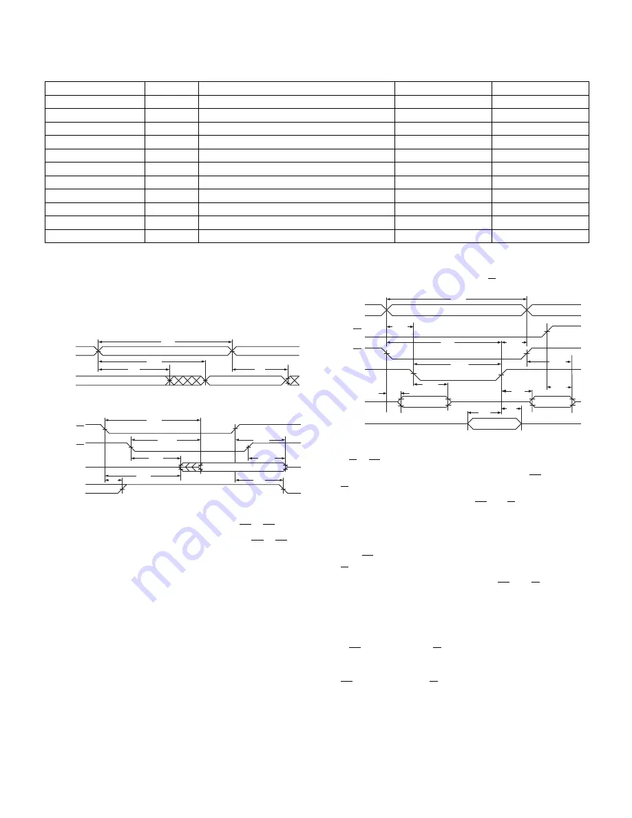
The access timing satisfies the dual-port SRAM specification.
• Timing Waveform of Read Cycle No. 1, Either Side
(1,2,4)
• Timing Waveform of Read Cycle No. 2, Either Side
(1,3)
NOTES:
1.
Timing depends on which signal is asserted last, OE or CE.
2.
Timing depends on which signal is de-asserted first, OE or CE.
3.
R/W = VIH.
4.
The start of valid data depends on which timing becomes effective,
tAOE, tACE or tAA
5.
tAA is for RAM Address Access and tSAA for is Semaphore
Address Access.
• Timing Waveform of Write Cycle No. 1, R/W Controlled Timing
(1,5,8)
NOTES:
1. R/W or CE must be HIGH during all address transitions.
2. A write occurs during the overlap (tEW or tWP) of a CE =VIL and R/
W = VIL.
3. tWR is measured from the earlier of CE or R/W going to VIH to the
end-of-write cycle.
4. During this period, the I/O pins are in the output state, and the input
signals must not be applied.
5. If the CE = VIL transition occurs simultaneously with or after the R/
W = VIL transition, the outputs remain in the High-impedance state.
6. Timing depends on which enable signal (CE or R/W) is asserted
last.
7. This parameter is guaranteed by device characterization, but is not
production tested. Transition is measured
m
500mV from the steady
state with the Output Test Load (Figure 2).
8. If OE = VIL during a R/W controlled write cycle, the write pulse
width must be the larger of tWP or (tWZ + tDW) to allow the I/O driv-
ers to turn off data to be placed on the bus for the required tDW. If
OE = VIH during an R/W controlled write cycle, this requirement
does not apply and the write pulse can be as short as the specified
tWP.
Signal name
I/O
Description
Connected to
Connection pin
A0~A11
I
Address Bus from host CPU
DP-RAM
A0R~A11R
D0~D7
I/O
Data Bus from host CPU
DP-RAM
D0R~D7R
/RD
I
Read signal from host CPU
DP-RAM
/OER
/WR
I
Write signal from host CPU
DP-RAM
R/WR
/DPCS
I
Chip select from host CPU
DP-RAM
/CER
/LRES
I
Rest signal for this board from host CPU
Board CPU
/RES
/INTSR
O
Data read end interrupt from board CPU
LOGIC
/INTSW
O
Data write end interrupt from board CPU
LOGIC
A13~A15
I
Address bus from host CPU (for decode)
LOGIC
Vcc
Power (+5V)
GND
GND
,
ADDRESS
DATA
OUT
PREVIOUS DATA VALID
DATA VALID
t
RC
t
AA
(5)
t
OH
t
OH
CE
OE
DATA
OUT
CURRENT
I
SB
ICC
50%
VALID DATA
(4)
50%
t
ACE
t
AOE
(4)
t
LZ
(1)
t
LZ
(1)
t
PU
t
HZ
(2)
t
HZ
(2)
t
PD
ADDRESS
R/W
DATA
OUT
DATA
IN
OE
CE
t
WC
t
AS
(6)
t
AW
t
WP
(2)
(4)
(4)
t
LZ
(7)
t
DW
t
DH
t
OW
t
HZ
(7)
t
HZ
(7)
t
WR
(3)
t
WZ
(7)
Summary of Contents for UP-3301
Page 91: ...UP 3301US PWB LAYOUT 89 CHAPTER 9 PWB LAYOUT 1 MAIN PWB A side ...
Page 92: ...UP 3301US PWB LAYOUT 90 B side 8 CUSTOMER DISPLAY PWB ...
Page 93: ...UP 3301US PWB LAYOUT 91 2 IR PWB 3 LCD PWB A Side B Side 4 INVERTER PWB A Side B Side ...
Page 94: ...UP 3301US PWB LAYOUT 92 5 MOTHER PWB 6 N F PWB 7 TOUCH PANEL PWB ...
Page 95: ...UP 3301US PWB LAYOUT 93 ...
Page 111: ......


