UP-3301US
CIRCUIT DESCRIPTION
– 52 –
2) DATA COMMUNICATION
Data is transmitted from the host CPU to the TCP/IP board or vice versa
through the dual-port SRAM. If data is written into the same address of
the dual-port SRAM from both sides or written into and read from the
same address from both sides, data is not assured. The following pro-
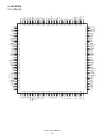
cedure should be observed.
The format of data to be handled should meet the software specifica-
tions.
• Interrupt signals from the host to board : Write/INTHW (Host Write),
Read/INTHR (Host Read)
/INTHW (Host Write) is generated by writing into the address H’7***
of the dual-port SRAM and cancelled by outputting the /HWACK sig-
nal by 100ns LOW pulse.
/INTHR (Host Read) is generated by reading the address H’B*** of
the dual-port SRAM and cancelled by outputting the /HRACK signal
by 100ns LOW pulse.
• Interrupt signals from the board to host : Write /INTSW (Slave Write),
Read /INTSR (Slave Read)
/INTSW (Slave Write) is generated by outputting the /SWRQ signal
by 100ns LOW pulse and cancelled by writing data into the address
H’B*** of the dual-port SRAM from the host side.
/INTSR (Slave Read) is generated by outputting the /SRRQ signal by
100ns low pulse and cancelled by reading data from the address
H’7*** of the dual-port SRAM.
7. LAN CONTROL
This board fixes RTL8019AS to the 8-bit mode on hardware.
The initial values of the items in the table are set as shown below by
hardware.
Any data loading EEPROM is not used. MAC address is written by the
CPU reading data on the flash memory and writing the register to the
LAN controller.
8. PORT SETTING
1
The common pins of the CPU are set as shown below.
Write
Y
N
Read
Y
N
Preceding data read
end interrupt?
Write data
Generation of write
end interrupt
Data write end
interrupt?
Read data
Generation of read
end interrupt
Item
Setting
Remarks
I/O Base Address
300H
IOS3~0=0,0,0,0
Network Media Type
TP/CX automatic
detection
PL1~0=0,0
BROM Size & Memory
Base Address
Disable
BS4~0=0,0,0,0,0
IRQ Select
INT0
IRQS2~0=0,0,0
Pin
No
I/O
Selection
signal
Remarks
2
I
PE15
/WP(FLASH write STATUS)
24
I
/IRQ0
Host write end interrupt (
4
Edge detection)
25
I
/IRQ1
Host read end interrupt (
4
Edge detection)
26
I
/IRQ2
Interrupt from LANC (
4
Edge detection)
28
I
/IRQ3
Reserve (
4
Edge detection)
29
O
A18
Address Bus
30
O
A19
Address Bus
31
I
/WAIT
wait from LANC
44
O
/CS3
Chip Select for LAN (Usual access space)
45
O
/CS2
Chip Select for dual-port SRAM
106
O
PE8
/SRRQ (Board side read end request)
107
O
PE9
/SWRQ (Board side write end request)
108
O
PE10
/HRACK
(host side read end interrupt cancel)
110
O
PE11
/HWACK
(host side write end interrupt cancel)
112
O
PE13
/RSTDRViActive Lowj
AEN
SA19-SA0
SD7-SD0
IORB
IOWB
INT0
IOCHRDY
CPU
RTL8019AS
SLOT16
GND
/CS3
A19-A0
D7-D0
/RD
/WRL
/IRQ2
/WAIT
Summary of Contents for UP-3301
Page 91: ...UP 3301US PWB LAYOUT 89 CHAPTER 9 PWB LAYOUT 1 MAIN PWB A side ...
Page 92: ...UP 3301US PWB LAYOUT 90 B side 8 CUSTOMER DISPLAY PWB ...
Page 93: ...UP 3301US PWB LAYOUT 91 2 IR PWB 3 LCD PWB A Side B Side 4 INVERTER PWB A Side B Side ...
Page 94: ...UP 3301US PWB LAYOUT 92 5 MOTHER PWB 6 N F PWB 7 TOUCH PANEL PWB ...
Page 95: ...UP 3301US PWB LAYOUT 93 ...
Page 111: ......


