background image

1 – 3

UX-A255U

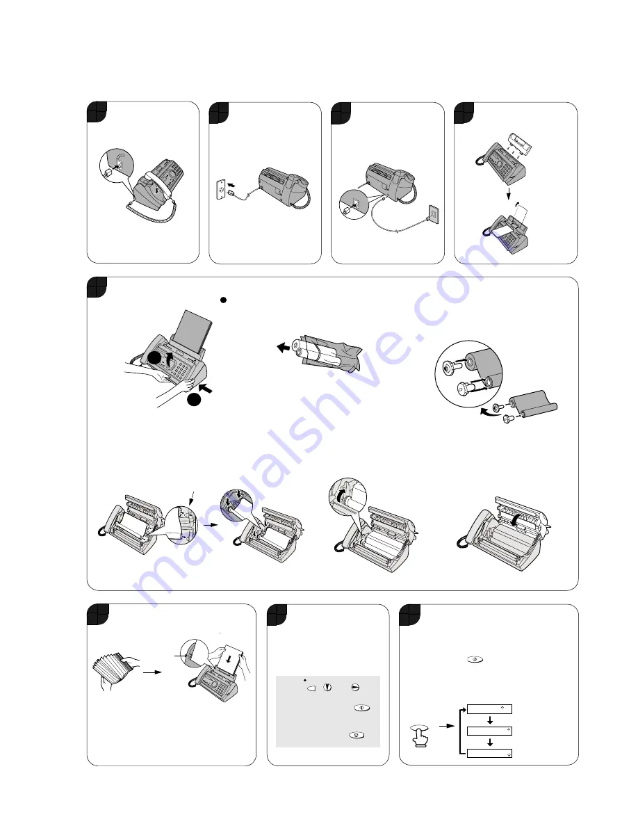
The stack

should not

be higher

than this line.

1

3

Plug the power cord
into a 120 V grounded
outlet.

Connect the telephone
line cord to the TEL. 
LINE
 jack and a wall
telephone jack.

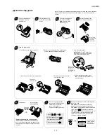
Attach the paper tray
and document support.

Load the imaging film.

1.Open the operation panel  (press     ).

3. Insert the green gears. 

IMPORTANT: Do NOT discard the
green gears. They are not included
with replacement imaging film.

Note: To enter your name and fax number and set the date and time so that they
appear at the top of each fax you send, see pages 16 - 19 of your operation
manual.

5

2. Remove the imaging film from its packaging. 

Cut the band that holds the rolls together.

2

Connect the handset
and place it on the
handset rest.

Note: If the
support does
not go in,
turn it over.

4. Insert the film into the print compartment.

5. Rotate the front spool as shown 

until the film is taut.

6. Close the operation panel (press 

down on both sides to make sure it 
clicks into place).

6

Load paper.

Note: If you loaded legal paper, see page 15 of the
operation manual to change the paper size setting
to LEGAL.

TEL

.

LIN

E

Fit ends of 
rolls onto hubs

1 slot

2 slots

Make sure 
the gears fit 
into the slots 
in the ends of 
the rolls.

Insert the paper
print side down.

4

• GENTLY LOAD PAPER INTO THE PAPER TRAY.

• DO NOT FORCE IT DOWN INTO THE FEED SLOT.

1

1

2

8

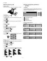
Select the reception mode for incoming faxes 
and voice calls:
FAX mode: The machine automatically 
answers all calls and begins fax reception.
TEL mode: Lift the handset when the machine 

rings. Press 

 to begin fax reception.

TAD mode: Select this mode when you go out 
to receive both voice messages and faxes. 
(Note: To select TAD mode, you must first 
record an outgoing message.)

START/MEMORY

The arrow in the 
display points to 
the selected 
reception mode.

RESOLUTION/

RECEPTION MODE

FAX

TEL

JAN-01 10:30

FAX

TEL

JAN-01 10:30

FAX

TEL

JAN-01 10:30

TAD

TAD

TAD

7

Record an outgoing message
(greeting) for TAD mode inviting
callers to leave a message.
(Note: "TAD" stands for
"Telephone Answering Device".)

1. Press 

, and 

.

2. Lift the handset, press 

and speak into the handset.

3. When finished, press 

.

REC/
MEMO

START/MEMORY

STOP

[5] Quick setup guide

Summary of Contents for UX-A255U

Page 1: ...n of CIS unit 5 13 CHAPTER 6 CIRCUIT SCHEMATICS AND PARTS LAYOUT 1 Control PWB circuit 6 1 2 TEL LIU PWB circuit 6 9 3 Power supply PWB circuit 6 14 4 Operation panel PWB circuit 6 16 5 Interface PWB circuit 6 18 CHAPTER 7 OPERATION FLOWCHART 1 Refer to the service manual of UX P100U 2 Refer to the service manual of UX P100U CHAPTER 8 OTHERS 1 Refer to the service manual of UX P100U 2 Refer to the...

Page 2: ...ohjeiden mukaisesti French ATTENTION Il y a danger d explosion s il y a remplacement incorrect de la batterie Remplacer uniquement avec une batterie du même type ou d un type recommandé par le constructeur Mettre au rébut les batteries usagées conformément aux instructions du fabricant Swedish VARNING Explosionsfare vid felaktigt batteribyte Använd samma batterityp eller en ekvivalent typ som reko...

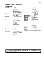
Page 3: ...paper Recording system Thermal transfer recording Halftone grayscale 64 levels Compression scheme MH MR MMR Display 16 digit LCD display Applicable telephone line Public switched telephone network Paper tray capacity Letter Approx 50 sheets 20 lb copier paper at room temperature maximum stack height should not be higher than the line on the tray Legal 5 sheets Recommended paper weight is 20 lb Cop...

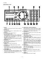
Page 4: ...N RECEPTION MODE key When a document is in the feeder press this key to adjust the resolution for faxing or copying At any other time press this key to select the reception mode an arrow in the display will point to the currently selected reception mode 11 FUNCTION key Press this key to followed by the arrow keys select special functions and setting 12 OpenLCR key Press this key to register for Op...

Page 5: ...er Note If you loaded legal paper see page 15 of the operation manual to change the paper size setting to LEGAL TEL LINE Fit ends of rolls onto hubs 1 slot 2 slots Make sure the gears fit into the slots in the ends of the rolls Insert the paper print side down 4 GENTLY LOAD PAPER INTO THE PAPER TRAY DO NOT FORCE IT DOWN INTO THE FEED SLOT 1 1 2 8 Select the reception mode for incoming faxes and vo...

Page 6: ...al the fax number 2 Press SPEAKER START MEMORY START MEMORY START MEMORY RESOLUTION RECEPTION MODE RESOLUTION RECEPTION MODE FAX TEL JAN 01 10 30 FAX TEL JAN 01 10 30 FAX TEL JAN 01 10 30 TAD TAD TAD START MEMORY FUNCTION START MEMORY A B C D E F G H I J K L M N O P Q R S T U V W X Y Z SPACE START MEMORY STOP 7 Option imaging film specifications UX 5CR 1 Structure This article is composed of polye...

Page 7: ... the limits below Output voltage settings 3 Settings 1 Dial mode selector DIAL mode Soft Switch No SW B4 DATA No 3 Output Voltage limits 5V 4 25V 5 75V 24V 23 3V 24 7V 2 IC protectors replacement ICPs IC Protectors are installed to protect the motor driver circuit ICPs protect various ICs and electronic circuits from an overcurrent con dition The location of ICPs are shown below 1 24V 2 24V 3 MG 4...

Page 8: ...ing 2 Diagnostics and service soft switch 1 Operating procedure 1 Entering the diagnostic mode Press FUNC 9 8 7 and the following display will appear ROM Ver TA18 After 2 sec DIAG MODE TA18 Then press the START key Select the desired item with the key or the key or select with the rapid key Enter the mode with the START key Diag specifications If the diag mode cannot be set repeat the diag mode op...

Page 9: ...s used to clear the backup memory and reset to the default settings 3 8 Shading mode The mode is used for the shading compensation For reading set up the special original paper The compensation memorizes the reference data of white and black for reading Moreover the memorized data is not erased even if memory clear mode is executed 3 9 All black print This mode is used to check the state of the pr...

Page 10: ...o finish the settings halfway between SW A1 and SW N3 press the STOP key In this case the setting being done to the SW No on display will be nullified while settings done to the preceding SW No remain in effect The soft switch mode is terminated S F T SW A1 0 0 0 0 0 0 0 0 START DATA No 1 2 3 4 5 6 7 8 When the COPY key is pressed the contents of soft switches are printed 4 How to make soft switch...

Page 11: ...unication error 0 sending mode reception 8 CNG transmission No Yes 0 CED tone signal interval 1000ms 750ms 500ms 75ms 1 No 1 1 1 0 0 0 2 No 2 1 0 1 0 0 3 MR coding No Yes 0 4 ECM mode No Yes 0 OPTION 5 ECM MMR mode No Yes 0 6 Reserved 0 7 Reserved 0 8 Reserved 0 1 Signal transmission level Binary input 0 2 No 16 8 4 2 1 1 3 1 2 3 4 5 0 4 0 1 0 0 0 0 5 0 6 Protocol monitor error print Printed at co...

Page 12: ... 0 6 No 6 0 1 0 1 0 7 Reserved 0 8 Reserved 0 1 Reserved 0 2 Reserved 0 3 Reserved 0 4 Reserved 0 5 Reserved 0 Auto dial mode delay timer of before line 0 second 1 5 seconds 3 0 seconds 4 5 seconds 6 connect No 6 0 0 1 1 0 7 No 7 0 1 0 1 0 8 Reserved 0 Auto dial mode delay timer of after line 1 7 seconds 3 0 seconds 3 6 seconds 4 0 seconds 1 connect No 1 0 0 1 1 0 2 No 2 0 1 0 1 0 3 Dial mode Tone...

Page 13: ...0 0 5 Automatic switching manual to auto receive Reception after 5 rings No reception 0 mode 6 Reserved 0 Cl detect frequency As PTT 11 5Hz 13 0Hz 20 0Hz 7 No 7 0 0 1 1 0 8 No 8 0 1 0 1 0 Distinctive ringing setting No 1 No 2 No 3 OPTION PATTERN 4 and 5 are for CANADA only OFF 0 0 0 STANDARD 0 0 1 PATTERN1 0 1 0 PATTERN2 0 1 1 1 PATTERN3 1 0 0 0 2 PATTERN4 1 0 1 0 3 PATTERN5 1 1 0 0 4 Reserved 0 5...

Page 14: ...on with GE telephone Compatible Not compatible 1 5 Remote operation code figure by external Binary input 0 6 TEL 0 9 No 8 4 2 1 1 7 5 6 7 8 0 8 0 1 0 1 1 1 CNG detection in STAND BY mode Yes No 1 OPTION Number of CNG detect AM mode 1pulse 2pulses 3pulses 4pulses 2 No 2 0 0 1 1 0 3 No 3 0 1 0 1 1 Number of CNG detect STAND BY mode 1pulse 2pulses 3pulses 4pulses 4 No 4 0 0 1 1 0 5 No 5 0 1 0 1 1 6 R...

Page 15: ...during OGM 8 Busy tone detect intermittent sound detect No Yes 0 Busy tone detection pulse number 2pulses 4pulses 6pulses 10pulses 1 No 1 0 0 1 1 0 2 No 2 0 1 0 1 1 3 Fax switching when A M full Yes No 0 OPTION 4 Busy tone detect continuation sound detect 320Hz 570Hz 320Hz 460Hz 0 frequency 5 Reserved 0 6 Reserved 0 7 AM OGM announce only mode Yes No 0 OPTION 8 Busy tone continuous sound detect ti...

Page 16: ... 1 0 0 1 AGC eref access code line Binary input 1 2 0 30 dB 2 dB step No 8 4 2 1 0 3 1 2 3 4 1 4 1 0 1 1 1 5 AGC eref access code Mic Binary input 1 6 0 30 dB 2 dB step No 8 4 2 1 1 7 5 6 7 8 0 8 1 1 0 1 1 1 AGC again adaptation threshold line Binary input 1 2 No 8 4 2 1 1 3 1 2 3 4 1 4 1 1 1 1 1 5 AGC again adaptation threshold Mic Binary input 1 6 No 8 4 2 1 1 7 5 6 7 8 1 8 1 1 1 1 1 AGC slew ra...

Page 17: ...munication results printout E T M Send only Always No print Err only OPTION 2 Transaction report No 2 0 0 0 0 1 1 3 No 3 0 0 1 1 0 0 4 No 4 0 1 0 1 0 0 5 OGM ICM output level to speaker Binary input 0 6 0 dB 15 dB 1 dB step No 8 4 2 1 0 7 5 6 7 8 1 8 0 0 1 1 1 1 Reserved 0 2 Reserved 0 3 OGM ICM output level Binary input 0 4 0 dB 32 dB 1 dB step No 32 16 8 4 2 1 0 5 3 4 5 6 7 8 1 6 0 0 1 0 0 1 0 7...

Page 18: ...No 32 16 8 4 2 1 0 3 1 2 3 4 5 6 0 4 0 0 0 0 1 0 0 5 1 6 0 7 Reserved 0 8 Reserved 0 1 LCR long time Binary input 0 OPTION 2 No 32 16 8 4 2 1 0 3 1 2 3 4 5 6 0 4 0 0 0 1 0 0 1 5 0 6 0 7 Reserved 0 8 Reserved 0 1 LCR Time Select Long Short 0 OPTION 2 Temporary release of caller ID withhold Yes No 1 3 Connect Japanese center Connect Japanese center Connect USA center 0 4 Open LCR debug mode Open LCR...

Page 19: ...set the function to print the content of HEADER PRINT described in the passcode list at the front end of receiver s original when original is sent to the remote machine If this switch is set to NO the HEADER PRINT is not output at the receiving machine SW A2 No 6 Reserved Set to 0 SW A2 No 7 Communication error treatment in RTN sending mode Reception Used to determine communication error treatment...

Page 20: ...al interval for speed and rapid dial calls Use a binary number to program this If set to 0 accidentally 1 will be assumed SW B1 No 5 No 8 Recall times Choice is made as to how many redials there should be SW B2 No 1 Dialing pause sec pause Pauses can be inserted between telephone numbers of direct dial con nection Selection of 4 sec or 2 sec pause is available SW B2 No 2 Dial tone detection before...

Page 21: ...tally receive ring is set to 1 NOTE If the machine is set to answer after a large number of rings it may not be able to receive faxes successfully If you have diffi culty receiving faxes reduce the number of rings to a maximum of 6 SW D1 No 5 Automatic switching manual to auto receive mode This soft switch is used to select whether the machine should switch to the auto receive mode after 5 rings i...

Page 22: ...700ms CI interruption 700ms Judged as a CI OFF section The section 1 is not judged as a CI OFF section the CI signal A is counted as one signal The section 2 is judged as a CI OFF section the CI signal B is considered as the second signal 00111 50ms 7 350ms CI interruption 350ms Judged as a CI OFF section The section 1 is judged as a CI OFF section and the CI signal A is counted as two signals The...

Page 23: ...en the average energy exceeds the AGC Gain Adaptation Threshold The AGC Gain Adaptation Threshold prevents message background noise from corrupting the gain provided that the AGC Gain Adaptation Threshold is greater than the background noise energy In the event that a message has background noise energy greater than the AGC Gain Adaptation Threshold the AGC Gain can be no greater than the AGC Maxi...

Page 24: ...1 No 6 A4 Paper enable The use of recording paper of A4 is enabled SW L1 No 7 LEGAL and LETTER paper enable The use of recording paper of LEGAL and LETTER is enabled SW L1 No 8 Reserved Set to 0 SW L2 No 1 No 2 Paper set size At present size of the recording paper SW L2 No 3 Automatic reduce of receive If set to 1 it is reduced automatically when receiving SW L2 No 4 No 6 Print contrast Used for a...

Page 25: ...SET SPEAKER 24V OPERATION PANEL TEL LIU PWB UNIT DRIVER MOTOR CONTACT IMAGE SENSOR DOCUMENT SENSOR PIO POWER SUPPLY PWB UNIT AMPLIFIER FAX MODEM DSP CORE SURGE PROTECT FILTER CML TRANSFORMER CI VBT STABILIZER RECTIFIER TRANSFORMER RECTIFIER DIODE TRANS SURGE ABSORBER FILTER LINE CLOCK 32 256MHz LCD FET THERMAL HEAD P IN SENSOR FILM SENSOR RECORDING PAPER FRONT SENSOR SIO S RAM 32kbit IA CX20438 CN...

Page 26: ...CNLCD OPERATION PANEL PWB NUIT 14 CNPN A 15 7 16 CNCSW CNMT CNTH CNCIS CNPN CNSP SPEAKER CNLIUA CNPW 14 6 CONTROL PWB UNIT TEL LIU PWB UNIT POWER SUPPLY PWB UNIT CNLIUA CNPS TEL LINE CNLNJ CNHJ AC CORD TX RX MOTOR 2 HANDSET 4 16 INTERFACE PWB CNPN A CNPN 2 Wiring diagram ...

Page 27: ...ED 24V VO VG CISVDD øT CISCLK GLED 24V KEN4A KEN3A KEN2A KEN1A DG 3 3V ORGSNS FRSNS E SEN0 SEN1 SEN2 SEN3 SEN4 SEN5 SEN6 CNPN CNCIS 1 2 3 4 5 6 7 8 9 10 11 12 13 14 1 2 3 4 5 6 7 8 9 10 11 12 13 14 TEL LIU PWB RHS MAG 24VL MICMUTE TELIN TELMUTE RXIN TXOUT CML PIN FILM CI HS TELOUT RHS MAG 24VL MICMUTE TELIN TELMUTE RXIN TXOUT CML PIN FILM CI HS TELOUT CNLIUA CNLIUA CNMT CNTH 1 2 3 4 5 6 1 2 3 4 5 ...

Page 28: ...he data is then converted from par allel to serial form by the modem where the serial data is modulated and sent onto the line Receive operation There are two ways of starting reception manual and automatic Depression of the START key in the off hook mode in the case of manual receive mode or CI signal detection by the LIU in the auto matic receive mode First the SCE214V controls the procedure sig...

Page 29: ...an be extened The ROM stores all the program object code 5 Flash Memory Controller The SCE214V includes a flash memory controller that supports NOR NAND and Serial NAND type flash memory The supported size of NOR type memory is up to 1 MB and the supported size of NAND type memory is unlimited 6 Stepper Motor Control Eight outputs are provided to external current drivers four to the scan ner motor...

Page 30: ...igh frequency as a modulation frequency the output level can be made programmable 18 Watchdog Timer The Programmable Watchdog Timer is intended to guard against firmware lockup on the part of either executive controlled background tasks or interrupt driven tasks and can only be enabled by a sequence of events under control of the Watchdog Control Logic Once the Watch dog Timer has been enabled it ...

Page 31: ...he modem The V 23 algorithm includes an optional programmable receive compromise equalizer which is active in both V 23 and Caller ID V 23 Receive only modes Common applications for V 23 include France s Minitel and Japan s Lowest Cost Routing 5 4 4 Features Group 3 facsimile transmission reception ITU T V 17 and V 33 ITU T V 29 V 27 ter T 30 V 21 Channel 2 T 4 ITU T V 17 and V 27 ter short train ...

Page 32: ... SIA The LSB of each 16 bit address contents is used to control the PIA The MSB of each 16 bit address contents is used to control the SIA The following table the PIA SIA control register RAM access code 5 5 Fig 3 PIA SIA Signal Flow Control Register SBRAMx BRx Crx IOx AREXx ADDx PIA Reg SIA Reg For changes made to IACR1 tobe effective the host must write to IAADD with a value of 0002h For changes...

Page 33: ... XIN I Osc1 30 XOUT O Osc1 31 WRPROTn O 1XC 32 TEST 1 I Hd 33 TEST 0 I Hd 34 BATRSTn I H 35 INTPWRDWNEn I H 36 PWRDWNn I O H 13Xs 37 N C 38 ADGA VADG PADC Analog GND 39 VREFn CLREF I VR PADC 40 VIN I VA PADC 41 ADGA VADG PADC Analog GND 42 ADVA VADV PADC Analog Power 43 ADXG VXG PADC 44 VREFp I VR PADC 45 VSS VSS Digital GND 46 IVREFn O VR PADC 47 IVREFp O VR PADC 48 VDD Digital Power 49 THADI I A...

Page 34: ...Digital GND 94 FCSn 1 VIDCTL 0 GPO 23 O 13Xs 95 IARESET O 13Xs DSP to EXTIA POR 96 IACLK O 13Xs DSP to EXTIA MCLK 97 VDD Digital Power 98 IA1CLK I H DSP from EXTIA ICLK 99 SR3IN DSPIRQn I H DSP from primary EXTIA SOUT EXT Modem IRQn 100 SR4OUT O 13Xs DSP to primary EXTIA SIN 101 SR1IO O 13Xs DSP to EXTIA CTRL1 102 SA1CLK I H DSP from EXTIA FSYNC 103 GPIO 7 SSRXD2 SASRXD2 I O Hu 13Xs 104 GPIO 6 SST...

Page 35: ...13Xs CPU Data Bus 146 D 5 I O Tu 13Xs CPU Data Bus 147 D 6 I O Tu 13Xs CPU Data Bus 148 D 7 I O Tu 13Xs CPU Data Bus 149 GPIO 20 ALTTONE I O Hu 13Xs 150 GPIO 26 I O Hu 13Xs 151 GPIO 27 I O Hu 13Xs 152 GPIO 28 I O Hu 13Xs 153 GPO 26 O 13Xs 154 GPO 27 O 13Xs 155 GPO 28 O 13Xs 156 GPO 29 O 13Xs 157 GPO 30 SR3OUT O 13Xs 158 GPIO 29 I O Hu 13Xs 159 GPIO 31 I O Hu 13Xs 160 GPIO 32 I O Hu 13Xs 161 VDD Di...

Page 36: ...CRYSTAL SCANNER CONTROLS SENSORS START CLK2 CLK1 CLK1N VIDCTL 1 0 XIN XOUT INTERNAL IA LINE INTERFACE DRAM SCANNER VIDEO PREPROCESSING SERIAL SYNC PORTS SSIF VIN VREFP VREFN SSCLK 2 1 SSTXD 2 1 SSRXD 2 1 SSSTAT 2 1 SYNC ASYNC SERIAL PORT SASIF SASCLK SASTXD SASRXD GPIO GENERAL PURPOSE I O DEBUGN VDD VDRAM VBAT VSS FLASH MEMORY OPTION WRPROTN FRDN FRWN FCLE FCSN 2 0 D 7 0 RDN A 23 0 WRN ROMCSN CS 5...

Page 37: ...is controlled by the combination of the attenuator value of the LINE DRIVER in the modem and the ringer sending level sent from the modem Speaker volume It is controlled by the attenuator value of the IC5 and IC3 VOL A B C 4 Ringer circuit section The ringer sound is formed in the tone of modem when CI signal is detected The amplifier circuit drives the speaker of the main body 5 10 DAC LPF DAC H ...

Page 38: ... 0 0 1 Level3 1 1 0 Level4 0 1 0 Level5 1 0 0 Ringer volume setting Low 1 1 1 Middle 0 0 1 High 0 0 0 DTMF speaker volume Level1 1 0 1 setting Level2 1 0 1 Level3 1 0 1 Level4 1 0 1 Level5 1 0 1 OGM playback speaker Level1 0 0 1 volume setting Level2 1 1 0 Level3 0 1 0 Level4 1 0 0 Level5 0 0 0 ICM record speaker Level1 0 0 1 volume setting Level2 1 1 0 Level3 0 1 0 Level4 1 0 0 Level5 0 0 0 Signa...

Page 39: ... CI DETECTOR SPEAKER LINE 24VL DG CONTROL PWB TEL LIU PWB RX TX TEL MUTE H MUTE PC1 Q101 IC7 IC102 A Q102 IC101 B Q105 Q104 IC101 A IC102 B IC5 0 1 0 0 1 0 1 1 RTLOOP ADC SIN MIC LINE SELECT MODEM BLOCK 20438 I A SP OUT ENABLE MIC ENABLE LINE IN ENABLE LINE OUT ENABLE 0 20 25 30dB LINESEL 1 1 0 0 1 0 0 4dB SOUT SPKRP MICP LINEIN LINE OUT MUTE 0 6 12dB IC3 SCE214V FAX CONTROLLER DTMFMUTE BZOUT1 RCV...

Page 40: ...Noise filter circuit The input noise filter section is composed of L1 and C1 which reduces normal mode noise from theAC line and common mode noise to the AC line 2 2 Rectifying smoothing circuit The AC input voltage is rectified by diode D1 2 3 4 and smoothed by capacitor C2 to supply DC voltage to the switching circuit section 2 3 Switching circuit This circuit includes MOS FET Q1 and the gate dr...

Page 41: ...5 D6 D7 A23 A22 A21 A20 A19 A18 A17 A16 A15 A14 A13 A12 A11 A10 A9 A8 A7 A6 A5 A4 A0 A3 A2 A1 RD WR ROMCS SYNC REGDMA GPO18 CLKDIV0 WAIT GPO19 CLKDIV1 RAS CAS DWR WRPROT BATRST VBAT PWRDWN INTPWRDOWNE XOUT XIN VREFp VREFn CLREF VIN THADI ALTTONE BZ OPI0 OPI1 OPI2 OPI3 SM0 SM1 SM2 SM3 OPO0 OPO1 OPO2 OPO3 OPO4 OPO5 OPO6 SXIN SXOUT CLK2 START STRB0 STRB1 STRB2 STRB3 PCLK PDAT PLAT VSS VSS VSS VSS VSS...

Page 42: ...C N C N C N C I O0 I O1 I O2 I O3 VSS VCC I O4 I O5 I O6 I O7 N C N C N C N C N C N C N C N C N C N C GND R B RE CE VCC N C N C N C N C IC1 SST39VF020P FLASH ROM 20 19 18 17 16 15 14 13 3 2 31 1 12 4 5 11 10 6 30 32 7 21 22 23 25 26 27 28 29 8 24 9 A0 A1 A2 A3 A4 A5 A6 A7 A8 A9 A10 A11 A12 A13 A14 A15 A16 A17 CE OE WE D0 D1 D2 D3 D4 D5 D6 D7 VDD GND N C A18 R125 10k R112 10k C100 0 1u 50V IC2 MSM5...

Page 43: ... 159 154 68 162 157 160 54 51 88 168 81 80 156 91 167 79 37 110 109 66 65 164 163 56 82 73 94 158 105 106 103 87 104 170 169 150 151 153 112 74 77 76 92 71 72 75 102 98 96 101 100 99 95 93 90 89 84 83 78 86 113 152 111 GPIO15 CS5 GPIO16 AVDD IIA GPIO37 GPO28 GPIO31 GPO27 GPO25 GPIO34 GPO30 GPIO32 GPIO13 GPIO17 SPKR_OUTP IIA GPO1 MIC_INM IIA MIC_INP IIA GPO29 MCDE0 GPO0 LINE_INP IIA N C SASRXD GPIO...

Page 44: ...K L102 0 R179 270 BAT1 CR2032 C211 470p 50V R103 270 REG1 814A33AUC BCX S 5 1 2 3 4 Vi n Vout VSS NC ON OFF R166 20k R127 51K R102 270 R100 5 6K R111 N M R168 270 C106 1000p 50V C171 100p 50V R170 N M C9 47u 25V C193 0 1u 50V R109 N M C10 22u 50V VBT1 C8 220u 6 3V C159 1u 10V VBT R147 N M C158 N M C192 0 1u 50V C157 N M DG DG CSWi ORGSNSi PWRDWN CNPN 8 CNPW 6 CNPW 5 CNPW 1 CNPW 2 CNPW 3 CNPW 4 CNP...

Page 45: ...149 100k R192 0 C114 0 1u 50V Q100 KTA1504GR B C E R152 20K R150 470K R171 120K C1 220u 6 3V IC6 KID65001AP 8 1 2 3 4 5 6 7 10 11 12 13 14 15 16 9 E 1B 2B 3B 4B 5B 6B 7B 7C 6C 5C 4C 3C 2C 1C COM Q102 KRC106 B C E VIN VO FU100 KAB2402 ZD1 1N4748 VG R163 0 1u 50V D1 D2 D3 D4 S1 S2 S3 G Q108 SI4431DY 4 5 8 3 1 2 6 7 C161 N M Q111 KRA102S B C E C160 1u 10V R151 100k C178 N M ZD100 02CZ18 Y R120 5 1K R...

Page 46: ...104 KRC102S B C E Q112 B C E R198 ZD101 N M C189 1u 10V R164 1M C214 R184 R180 39K R194 IC10A 4 5 3 9 7 6 8 16 IC10B 15 1 2 10 7 6 8 16 C2 47u 25V 1 2 C187 0 1u 16V K R143 39K R181 R144 24K C182 1u 10V K C183 IC11 2 1 5 3 4 C181 0 R140 470K R138 N M R142 200K C216 R122 100K C156 0 1u 50V C186 0 C125 1u 10V R146 91K R193 0 C150 1u 10V R203 R136 3K R196 R201 C213 R145 6 2K C185 R124 220K R131 15K IC...

Page 47: ...UX A255U Control PWB parts layout Top side 6 7 ...

Page 48: ...UX A255U Control PWB parts layout Bottom side 6 8 ...

Page 49: ... 1SS133 JP24 R145 REC1 R143 R10 Q 4 AR2 ERZV5D471 C20 0 01 N M R144 L7 N M ZD6 JUMPER JP25 L4 JP20 N M R9 C122 T1 I2164 JP21 N M PC1 1 2 PC817X4 PC4 1 2 AR1 ERZV5D471 L8 PC2 1 2 A R5 JP1 C125 ZD4 HZ27 A JP4 Vref A C118 DG ARG CNTLJ 3 CNLNJ 3 CNTLJ 2 CNLNJ 4 CNLNJ 1 CNLNJ 2 CNLNJ 6 CNLNJ 5 CNTLJ 4 CNTLJ 5 4 3 G G 9 8 10 4 5 3 2 1 2 1 4 3 2 5D L2 E S EX T2 EX T1 N C E S L1 T1 T2 2 5D NOTE These mark...

Page 50: ...A Q102 KRC106S C127 0 R126 Vref B C22 N M ZD7 MTZJ10B Vref A R104 3 3K IC102 NJM2904M C138 N M IC101 NJM2904M C129 N M Q6 KRA102M Vref A Q106 N M JP29 N M C4 22 50 2 3D JP30 N M R107 1K C1 22 50 JP31 C143 0 C112 2200P N M A R132 0 IC101 NJM2904M C144 1 C100 N M IN OUT R120 3 3K R125 1K C145 1 R112 1 5K C139 33P R127 0 R110 13K DG1 C106 N M C105 N M R124 620 R100 3 3K Q101 KRC106S E D1 C137 820P L3...

Page 51: ...3 Vref A C111 0 1 PC2 2 2 C3 IC101 NJM2904M PC4 2 2 N M R116 DG1 CML 3 3 OUAZ SH 124DZ Q109 N M HSDG PH2 SG206 Vref A R123 Vref A R129 24VA R113 0 TP2 C120 0 1 24VL C14 22 50 SW1 HOOK SW R108 DG DG DG DG DG DG DG DG DG DG DG DG DG CNLIUA 11 CNLIUA 13 CNLIUA 2 CNLIUA 9 CNLIUA 3 CNLIUA 17 CNLIUA 15 CNLIUA 12 CNLIUA 10 CNLIUA 16 CNLIUA 1 Vout 1 GND 2 Vin 3 2 1 4 3 8 4 2 1 8 4 4 3 3 1 2 RHS 24VL DG PI...

Page 52: ...UX A255U TEL LIU PWB parts layout Top side 6 12 ...

Page 53: ...UX A255U TEL LIU PWB parts layout Bottom side 6 13 ...

Page 54: ... 3SB2 T1 C6 0Ω D5 1SS355TE R6 PC1 PS2501 1L 1 2 C17 C5 0 015 R7 180 D6 12 3 1 5 4 11 14 15 R2 470K R3 470K Q1 FS7KM C3 1000P ZD1 RD27ESAB2 Q2 2SC4115S Q3 2SC1741AS R9 47 R10 0 12 1W R8 47K C26 C27 CNAC F1 2 5A 125V C1 2 2 C7 0 01 C28 0 01 R1 2 2M 1 2W 1 2 V1 S07K150GA L1 19mH 0 5A D2 ERA15 06 D4 ERA15 06 D3 ERA15 06 D1 ERA15 06 N M CNPS 1 2 3 4 5 6 24V 24V MG 24V GND MG 24V GND Vreg 5V DG Vreg GND...

Page 55: ...UX A255U Power supply PWB parts layout Top side 6 15 Power supply PWB parts layout Bottom side ...

Page 56: ...N5 CNPN_A 10 CNPN_A 11 CNPN_A 13 CNPN_A 14 CNLCD 11 CNLCD 12 CNLCD 13 CNLCD 14 CNLCD 4 CNLCD 5 CNLCD 6 CNLCD 3 CNLCD 2 CNLCD 1 CNPN_A 3 CNPN_A 2 CNPN_A 1 CNPN_A 4 CNPN_A 15 CNPN_A 16 CNPN_A 9 CNPN_A 6 CNPN_A 5 CNPN_A 7 CNPN_A 8 CNPN_A 12 N M 2 6 11 14 4 12 8 LD2 N C N C LD0 E 1 3 5 7 9 10 13 N C LD1 LD3 N C R W DG RS VO 3 3V CNPN 2 6 11 14 4 12 16 8 SEN3 ORGSNS E SEN1 3 3V 1 3 5 7 9 10 13 15 SEN0 ...

Page 57: ...UX A255U 6 17 Operation panel PWB parts layout Top side Operation panel PWB parts layout Bottom side Note Since the parts of PWB cannot be supplied change it as a unit ...

Page 58: ...A CNPN A SEN6 SEN0 SEN1 SEN2 SEN3 SEN4 SEN5 KEN1A KEN2A E 3 3V ORGSNS FRSNS DG KEN4A KEN3A KEN4A KEN3A KEN2A KEN1A ORGSNS FRSNS E SEN0 SEN1 SEN2 SEN3 SEN4 SEN5 SEN6 DG 3 3V CNPN A 10 CNPN A 11 CNPN A 13 CNPN A 14 CNPN A 15 CNPN A 16 CNPN A 12 CNPN A 3 CNPN A 4 CNPN A 9 CNPN A 6 CNPN A 5 CNPN A 7 CNPN A 8 CNPN A 1 CNPN A 2 CNPN 10 CNPN 11 CNPN 12 CNPN 3 CNPN 4 CNPN 9 CNPN 5 CNPN 7 CNPN 8 CNPN 1 CNP...

Page 59: ... with the parts specific to the product specification 1 Cabinet etc 2 Top cover Sub frame 3 Upper cabinet Document guide upper 4 Drive unit 5 Packing material Accessories 6 Control PWB unit 7 TEL LIU PWB unit 8 Power supply PWB unit 9 Operation panel PWB unit 10 Interface PWB unit Index UX A255 MODEL SELECTION CODE DESTINATION UX A255U U S A ...

Page 60: ...OCUMENT GUIDE UPPER TOP COVER SUB FRAME DRIVE UNIT 62 27 22 30 31 28 25 26 26 29 4 57 35 54 46 50 52 51 53 56 3 5 36 37 58 48 47 8 6 60 17 49 41 42 45 55 39 38 39 40 7 61 44 43 59 29 25 24 33 34 32 63 23 16 64 65 B2 B1 B1 B1 B1 B1 B1 B2 B3 B2 W1 B4 ...

Page 61: ...AB C Head spring A 39 MSPRC3288XHZZ AB C Head spring B 40 MSPRC3340XHZZ AD N C Head spring C 41 PCOVP2130XHZZ AE C Head cover 42 PGIDM2615XHZZ AD C Head guide left 43 PGIDM2616XHZZ AD C Head guide right 44 QCNWN486AXHZZ AM C Head cable 45 RHEDZ2065XHZZ BP B Thermal head 46 GCOVA2447XHSA AF D Front cover 47 GLEGG2078XHZZ AD C Rubber leg 48 LPLTM3178XHZZ AF C Bottom plate 49 LPLTP3177XHZZ AD C Stopp...

Page 62: ...7XHZZ AG C Paper feed roller shaft 16 NSFTP2358XHZZ AG C PU roller shaft 17 PGIDM2621XHSA AF C Release lever 18 LHLDZ2224XHZZ AL C RP feed plate holder 19 LPLTG3181XHZZ AD C RP separate rubber 20 LPLTP3179XHZZ AD C RP separate base 21 LPLTP3180XHZZ AH C RP separate plate 22 LPLTP3182XHZZ AH C RP feed plate 23 MSPRC3299XHZZ AB C RP separate spring 24 MSPRC3300XHZZ AB C RP feed spring 25 LBSHP2141XH...

Page 63: ...6AXZZ AH C FRSNS sensor SW1 1 8 QSW M2294XHZZ AE C ORGSNS sensor SW2 9 QCNWN487AXHZZ AL C Panel cable 10 RUNTZ2080XH01 BA E LCD unit 11 LPLTG2911XHZZ AE C Separate rubber 12 LPLTP3175XHZZ AD C Separate plate 13 LPLTP3176XHZZ AD C Feed plate 14 MSPRD3293XHZZ AB C Separate spring 15 MSPRT3294XHZZ AB C Feed spring 16 PGIDM2614XHSA AL C Document guide upper 17 PSHEP3660XHZZ AE C Separate rubber sheet ...

Page 64: ...D3298XHZZ AE C Cam hold spring 10 NGERH2380XHZZ AC C Reduction gear 17 36Z 11 NGERH2409XHZZ AB C Idler gear 23Z 12 NGERH2571XHZZ AD C Slip gear 13 NGERH2572XHZZ AD C Reduction gear 25 63Z 14 NGERH2573XHZZ AD C Reduction gear 20 40Z 15 NGERH2574XHZZ AD C Reduction gear 15 30Z 16 NGERH2575XHZZ AD C Idler gear 40Z 17 NGERH2576XHZZ AD C Idler gear 21Z 18 NGERH2577XHZZ AD C Idler gear 20Z 19 NGERH2582X...

Page 65: ...cord 7 TCADZ3319XHZZ AT N D Setup guide 8 TCADZ3283XHZZ AD D Fax transmission sheet 9 TCADZ3282XHZZ AD D Open LCR information 11 TINSE4265XHTZ AT N D Operation manual 12 TLABM309DXHZZ AD N D Pop label 14 SPAKA465CXHZZ AF D Packing add left 15 SPAKA466CXHZZ AF D Packing add right 16 SPAKA467CXHZZ AD D Packing add accessories 17 CPAKC292DXH01 AV N D Packing case with label 18 SPAKP474CXHZZ AB D Viny...

Page 66: ...YCY1HF104Z AA C Capacitor 50WV 0 1µF C139 39 VCKYCY1AF105Z AC C Capacitor 10WV 1µF C140 40 VCKYCY1HF104Z AA C Capacitor 50WV 0 1µF C141 41 VCKYCY1AF105Z AC C Capacitor 10WV 1µF C142 42 VCKYCY1AF105Z AC C Capacitor 10WV 1µF C143 43 VCKYCY1AF105Z AC C Capacitor 10WV 1µF C144 44 VCKYCY1AF105Z AC C Capacitor 10WV 1µF C145 45 VCCCCY1HH200J AA C Capacitor 50WV 20PF C146 46 VCKYCY1AF105Z AC C Capacitor 1...

Page 67: ...103J AA C Resistor 1 16W 10KΩ 5 R101 121 VRS CY1JB271J AA C Resistor 1 16W 270Ω 5 R102 122 VRS CY1JB271J AA C Resistor 1 16W 270Ω 5 R103 123 VRS CY1JB000J AA C Resistor 1 16W 0Ω 5 R104 124 VRS CY1JB471J AA C Resistor 1 16W 470Ω 5 R105 125 VRS CY1JB471J AA C Resistor 1 16W 470Ω 5 R106 126 VRS CY1JB103J AA C Resistor 1 16W 10KΩ 5 R107 127 VRS CY1JB471J AA C Resistor 1 16W 470Ω 5 R108 128 VRS CY1JB10...

Page 68: ...95 RCRSP2176SCZZ AG B Crystal 32 256MHz X1 196 RCRSB0297AFZZ AD B Crystal 32 768kHz X2 197 VHE1N4748A 1 AC B Diode 1N4748A ZD1 198 VHE02CZ180Y 1 AC B Zener diode 02CZ180Y ZD100 Unit 901 DCEKC282RXHZZ BU N E Control PWB unit Within ROM 7 TEL LIU PWB unit 1 VHVERZV5D471 AC B Varistor ERZV5D471 AR1 2 VHVERZV5D471 AC B Varistor ERZV5D471 AR2 3 VCEAGA1HW226M AB C Capacitor 50WV 22µF C1 4 VCEAGA1HW226M ...

Page 69: ...6W 22KΩ 5 R133 74 VRS CY1JB243J AA C Resistor 1 16W 24KΩ 5 R134 75 VRS CY1JB153J AA C Resistor 1 16W 15KΩ 5 R135 76 VRS CY1JB393J AA C Resistor 1 16W 39KΩ 5 R136 77 VRS CY1JB332J AA C Resistor 1 16W 3 3KΩ 5 R137 78 VRS CY1JB822J AA C Resistor 1 16W 8 2KΩ 5 R142 79 VHINJM78L05A1 AD B IC NJM78L05A REG1 80 QSW Z2317XHZZ AF C Hook switch SW1 1 81 RTRNI2164XHZZ AG B Transformer I2164 T1 82 VHVRA391PV6 ...

Page 70: ...Resistor 1 8W 330KΩ 5 R15 47 0CBUEXCAP103 AC C Resistor 1 8W 10KΩ 5 R16 48 0CBUEXCAP332 AC C Resistor 1 8W 3 3KΩ 5 R17 49 0CBUEXJAV332 AC N C Resistor 1 4W 3 3KΩ 5 R18 50 0CBUDXDAW682 AC N C Resistor 1 4W 6 8KΩ 5 R27 51 0CBUDXDAW682 AC N C Resistor 1 4W 6 8KΩ 5 R28 52 0CBUDXDAW682 AC N C Resistor 1 4W 6 8KΩ 5 R29 53 0CB829655050 BF N B Transformer PTTN129 KTT T1 54 0CBUEZ0666ZZ AD B Varistor S07K1...

Page 71: ... 27 AD C NGERH2580XHZZ 2 11 AC C NGERH2581XHZZ 2 12 AC C NGERH2582XHZZ 4 19 AC C NGERP2318XHZZ 2 3 AD C NROLP2332XHZZ 1 29 AD C NROLR2482XHZZ 1 30 AR C NROLR2483XHZZ 2 13 AL C NROLR2484XHZZ 2 14 AL C NROLR2485XHZZ 2 28 AQ C NSFTP2357XHZZ 2 15 AG C NSFTP2358XHZZ 2 16 AG C P PBRS 2055XHZZ 1 63 AN C PCOVP2130XHZZ 1 41 AE C PCOVP2131XHSA 1 57 AD C PCOVP2132XHZZ 1 58 AD C PGIDM2614XHSA 3 16 AL C PGIDM2...

Page 72: ... 6 126 AA C 6 128 AA C 6 138 AA C 6 165 AA C VRS CY1JB104J 6 136 AA C 6 158 AA C 6 160 AA C VRS CY1JB105J 6 145 AA C 6 168 AA C VRS CY1JB106J 6 166 AA C VRS CY1JB124J 6 173 AA C VRS CY1JB133J 7 60 AA C VRS CY1JB150J 6 110 AA C VRS CY1JB151J 6 131 AA C 6 185 AA C 6 186 AA C VRS CY1JB152J 7 62 AA C VRS CY1JB153J 6 143 AA C 7 75 AA C VRS CY1JB154J 6 135 AA C VRS CY1JB155J 6 152 AA C VRS CY1JB163J 7 5...

Page 73: ... AC C 0CBUEXCAP102 8 45 AC C 0CBUEXCAP103 8 47 AC C 0CBUEXCAP181 8 40 AC C 0CBUEXCAP272 8 39 AC C 0CBUEXCAP332 8 48 AC C 0CBUEXCAP334 8 46 AC C 0CBUEXCAP470 8 42 AC C 0CBUEXCAP472 8 44 AC C 0CBUEXCAP473 8 41 AC C 0CBUEXDAW474 8 36 AC N C 8 37 AC N C 0CBUEXJAV332 8 49 AC N C 0CBUEZ0666ZZ 8 54 AD B 0CBUFBA222EQ 8 55 AD B 0CBUGA0291ZZ 8 2 AC C 0CBUGA0302ZZ 8 9 AK N C 0CBUGA0315ZZ 8 8 AL N C 0CBUGCM10...

Page 74: ...92 Japan Printed in U S A A0112 1124DS IS T No part of this publication may be reproduced stored in a retrieval system or transmitted in any form or by any means electronic mechanical photocopying recording or otherwise without prior written permission of the publisher COPYRIGHT 2001 BY SHARP CORPORATION ALL RIGHTS RESERVED ...

Reviews: