51
VC-S101U
V
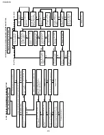
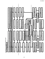
ideo recording possible, but no color output (possible in E-E mode)
Is chroma signal fed to pin (18) of IC201?
Is chroma signal fed to pin (17) of IC201?
Is chroma signal fed to pin (77) of IC201?
Is chroma signal fed to pin (76) of IC201?
Is chroma signal fed to pin (80) of IC201? Is signal level as
specified (about 460 mVp-p burst)?
Is chroma signal fed to pin (3) of record current adjustment
circuit (IC206)?
Is chroma signal fed to pin (30)(TP308) of H/A
circuit (IC301)?
Check the line between pin (3) of record current adjustment
circuit (IC206) and pin (30)(TP308) of IC301.
Replace IC201.
Replace IC201.
Replace IC201.
Check C515.
Is 5V voltage applied to pin (78)(C.Vcc) of IC201?
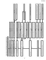
Check C250.
Check pins (1
1) and (13) of IC201 as well as the peripheral
circuits of X501.
Are there signals of about 3.58 MHz/500 mVp-p and of
3.58 MHz/1.2 Vp-p at pins (1
1) and (13) of IC201,
respectively?
Is there VCO signal of about 8.4 MHz/600 mVp-p at pin (7)
of IC201?
Check the peripheral circuits of pin (7) of IC201.
Check the record current adjustment circuit (IC206) between
pin (80) of IC201 and pin (3) of IC206.
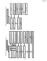
Is record control voltage (about 2.7 Vdc) applied from pin (4)
of adjustment voltage supply IC (IC203) to pin (2) of IC206?
Is reference voltage of adjustment voltage supply IC (IC203)
as specified? (4.4 V at pin (1
1) and 2.8 V at pin (13))
Are there IIC clock and IIC data signals fed to pins (2) and
(3) of adjustment voltage supply IC (IC203)?
Check the EEPROM (IC704). Reprogram as required.
Check the PC 5V(2) line.
Check the peripheral circuits of adjustment peak voltage
setting circuits (IC207, IC208). Replace as required.
Check IC206. Replace as required.
Check the line between pins (2) as well as (3) of IC203 and
pins (18) and (17) of IC701.
Replace the EEPROM (IC704).
YES
YES
YES
YES
YES
YES
NO
NO
NO
NO
NO
NO
NO
NO
NO
NO
YES
YES
YES
YES
YES
YES
YES
NO
NO
NO
NO
NO
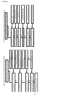
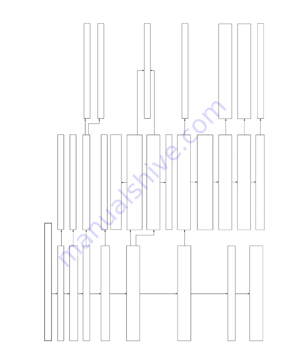
FLOW CHART NO.21 RECORDING MODE TROUBLESHOOTING (2)
Summary of Contents for VC-S101U
Page 6: ...VC S101U 6 1 3 LOCATION OF MAJOR COMPONENTS AND CONTROL ...
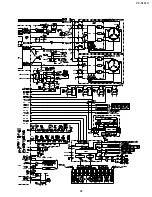
Page 58: ...58 VC S101U 8 BLOCK DIAGRAM SYSTEM SERVO BLOCK DIAGRAM ...
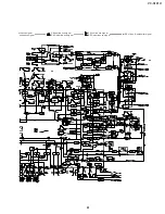
Page 59: ...59 VC S101U ...
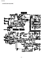
Page 60: ...60 VC S101U SIGNAL FLOW BLOCK DIAGRAM REC Luminance signal REC Chrominance signal ...
Page 62: ...62 VC S101U AUDIO BLOCK DIAGRAM ...
Page 63: ...63 VC S101U REC Signal PB Signal EE Signal ...
Page 64: ...64 VC S101U POWER CIRCUIT BLOCK DIAGRAM ...
Page 67: ...67 13 12 11 10 9 8 7 VC S101U ...
Page 69: ...69 13 12 11 10 9 8 7 VC S101U ...
Page 71: ...71 13 12 11 10 9 8 7 VC S101U ...
Page 73: ...73 13 12 11 10 9 8 7 VC S101U ...
Page 75: ...75 13 12 11 10 9 8 7 VC S101U ...
Page 77: ...77 13 12 11 10 9 8 7 VC S101U ...
Page 79: ...79 13 12 11 10 9 8 7 VC S101U ...
Page 81: ...81 13 12 11 10 9 8 7 VC S101U ...
Page 83: ...83 13 12 11 10 9 8 7 VC S101U ...
Page 84: ...84 7 6 5 4 3 2 1 A B C D E F G H VC S101U PWB FOIL PATTERN MAIN PWB ...
Page 85: ...85 13 12 11 10 9 8 7 VC S101U ...
Page 86: ...86 7 6 5 4 3 2 1 A B C D E F G H VC S101U Y C PWB SIDE A Y C PWB SIDE B ...
Page 87: ...87 13 12 11 10 9 8 7 VC S101U NR PWB SIDE A NR PWB SIDE B ...
Page 88: ...88 7 6 5 4 3 2 1 A B C D E F G H VC S101U Hi Fi JACK PWB SIDE A SIDE B ...
Page 89: ...89 13 12 11 10 9 8 7 VC S101U OPERATION PWB FRONT A V PWB ...
Page 90: ...90 7 6 5 4 3 2 1 A B C D E F G H VC S101U JACK PWB SIDE A JACK PWB SIDE B ...


