background image

2. HARDWARE DESCRIPTION

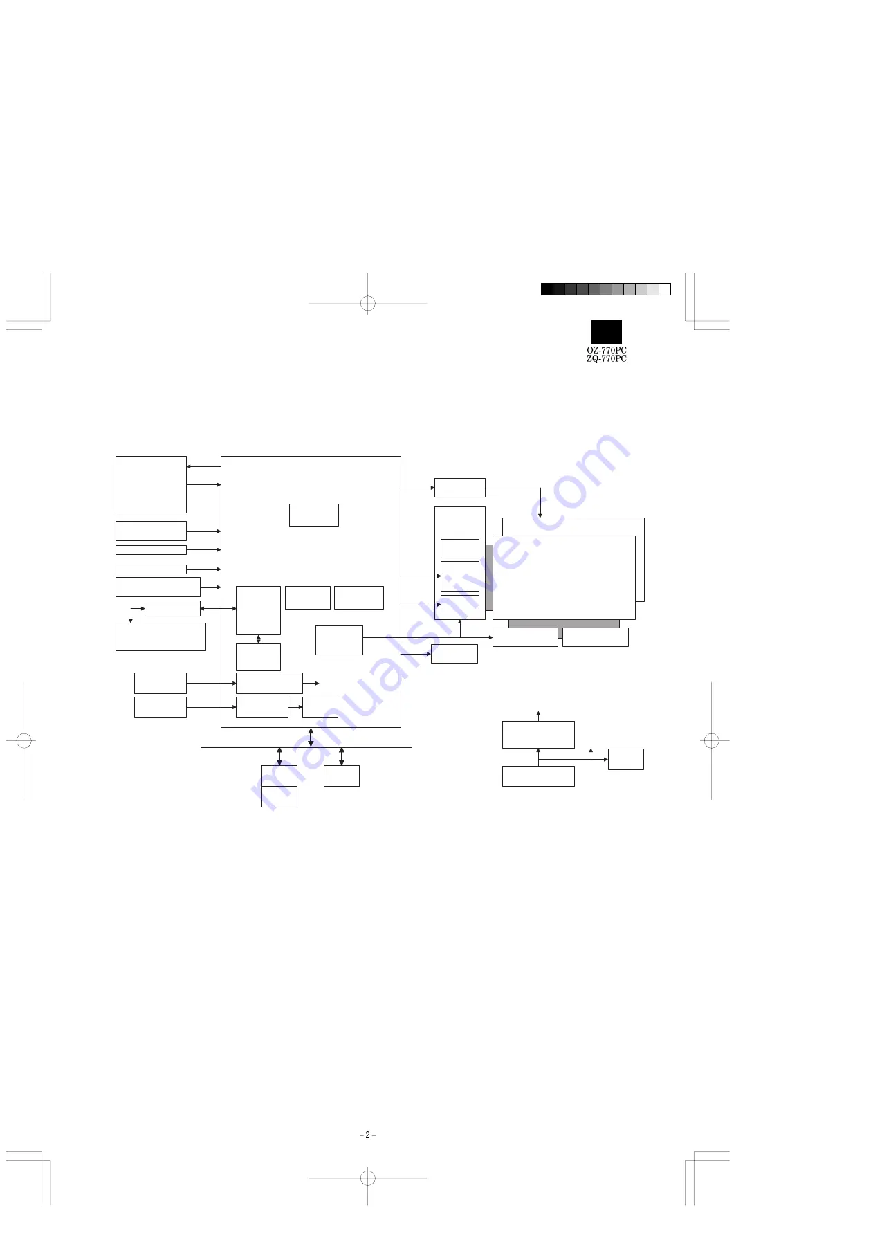
1. Block diagram

2-1. CPU (T5L55) : COB (Bare Chip) is used

1) Features

Microcontroller T5L55 is a revised version of T6B31

Added/revised functions of T5L55 compare to T6B31 are follows.

1. IrDA1.0 encorder/decorder circuit is integrated.
2. 120 segment LCD driver controller function is aclded.
3. LCD refresh frequency is revised.
4. Some gate circuits such as the interrupt circuit, the reset circuit

and the latch circuit are added.

The chip has 100 pads. The pad pitch is 150um, and is as same
as T6B31.

Operating voltage : VDD = +4.5 ~ +5.5V

2-2. LCD driver (JT6J14-AS) : COB 

(Bare Chip ) is used

The JT6J14-AS is an 120-channel-output column driver for an STN
dot matrix LCD. The JT6J14-AS features 28-V LCD drive voltage and
a 10-MHz maximum operating frequency. The JT6J14-AS is able to
drive LCD panels with a duty ratio of up to 1/160.

1) Features

Display duty application:

to 1/160

LCD drive signal:

120

Data transfer:

4-bit bidirectional

Maximum Operating frequency: 10 MHz (V

DD

 = 4.5 V),

6.5 MHz (V

DD

 = 2.7 V)

LCD drive voltage:

11 to 28 V
(maximum drive voltage = 30 V)

Power supply Operating voltage: 2.7 to 5.5 V

Operating temperature:

–20 to 75°C

LCD drive output resistance:

2.2 k

 (max)

(12.8 V, 1/7 to 1/14 bias)

Display-off function:

When /DSPOF is L, all LCD drive out-
puts (O1 to O120) remain at the V

SS

/V5

level.

Low power consumption: Cascade connections and auto enable

transfer functions are available.

Key Board

Matrix

Battery Replacement

Switch

Reset Switch

Power ON Button

Main Battery Voltage

Detection

CPU JT5L55

CPU core

Z80

Level Converter

4P Serial Communications

Port

(for PC synchronize)

9.8304MHz

X'tal

32.768kHz

X'tal

Main Clock

RTC

Clock

Oscillator

Main Clock

Oscillator

IrDA

Encoder

/Decoder

Serial

Interface

Interrupt

Controller

Chip Select

Controller

LCD

Controller

FROM
16Mbit

FROM

8Mbit

SRAM

1Mbit

Vcc

Vbatt

Voltage

Detector

Power Conversion

(5.0V Step Up)

Main Batteries

(LR6 x 2)

Piezo Electric

Buzzer

Step Up

Segment Driver

120 segment

Segment Driver

120 segment

LCD

239seg x 80com

Contrast

Adjust

LVC

Common

Driver

80 common

EL Driver

EL Backlight

Summary of Contents for Wizard OZ-770PC

Page 1: ...ition subtraction multiplication division constant memory calculation conversion calculation Clock Crystal oscillation frequency 32 768 Hz Accuracy Average variance per day 2 0 seconds at 25 C 77 F Display information year month day day of the week hours minutes A M P M city names Time system 12 hour and 24 hour Other function Display of date and time for various cities around the world Enable dis...

Page 2: ...th of time Power key Turns on and off the unit Display Shows information and is used for navigating the various functions Application keys Starts appropriate applications Backlight key Reset button Initializes and resets the Organizer Battery replacement switch Locks the battery compartment to prevent access to the batteries Operating battery compartment Holds operating batteries 4 pin Cable Jack ...

Page 3: ...directional Maximum Operating frequency 10 MHz VDD 4 5 V 6 5 MHz VDD 2 7 V LCD drive voltage 11 to 28 V maximum drive voltage 30 V Power supply Operating voltage 2 7 to 5 5 V Operating temperature 20 to 75 C LCD drive output resistance 2 2 kΩ max 12 8 V 1 7 to 1 14 bias Display off function When DSPOF is L all LCD drive out puts O1 to O120 remain at the VSS V5 level Low power consumption Cascade c...

Page 4: ...1CP is a 131 072 word x 8 bit 5 V driven asynchronous high speed CMOS static RAM The power consumption is 5mA MHz standard in operation and the access time is a maximum of 5ns that is the use of a new circuit has turned high speed and low power consumption into reality In addition the power consumption is only 1µA in standby state and data can be backed up by the battery 2 Features Low power consu...

Page 5: ...SS GND TERMINAL VOUT OUTPUT TERMINAL 3 Memory mapping CHIP SELECT DESCRIPTION SIZE CE1 FLASH ROM PROGRAM DATA 16Mbit CE3 CE4 CE5d CE RAMd SRAM 1Mbit CE7 CE8 4 Power circuit Explanation of the power source name Normal VCC5 0V System LSI power 5 0V VBAT Battery voltage 3 0V GND reference voltage 0V Supply of the operating power LR6 alkaline battery x 2 The operating voltage main battery of 3V 1 5V x...

Page 6: ...ts to remember when installing new batteries Replace the two operating batteries at the same time with new batter ies of the same type Caution Keep batteries out of the reach of children Remove batteries from the unit when they become weak or when the unit will not be used for a long period of time Leaving weak batteries in the unit may cause battery leakage and damage from corrosion Do not dispos...

Page 7: ...s replaced 2 When the FLASH ROM is replaced 3 When the following functions are carried out from the Diag Check 1 5 FINAL check page 1 5 2 5 AGING page 2 5 3 1 FLASH ROM CLEAR page 5 5 1 Necessary devices 1 PC Windows 95 98 or Windows NT 4 0 2 Docking module 3 RE PROGRAM software for PC EO8RPRxxxx exe xxx shows the version number The software on the machine side is included in this software When th...

Page 8: ...ey Push all key 45 hex different characters and the no of keys are displayed When push a key one of corresponding characters will be disappeared and the no of key will be decrement by one Keyboard will be OK only if all characters had been disappeared after all keys had been pressed 5 Backlight check Push 4 key BackLight is on no indication on time 30sec 6 Low Battery Check Push 6 key Drop the ope...

Page 9: ...TO SHEET 4 FPCB TO SHEET 5 FROM SHEET 4 The SW open when the door is locked TO SHEET 4 TO SHEET 3 FROM SHEET 4 TO SHEET 5 2 2uF 5 CIRCUIT DIAGRAM AND PARTS LAYOUT 1 Main PWB Circuit 1 CPU ...

Page 10: ...2 Memory FROM SHEET 2 FROM SHEET 2 FROM SHEET 4 FROM SHEET 2 TSOP TSOP LHF08CH1 U12 is not mounted Trace only ...

Page 11: ...3 4pin EM3 MMZ2012D301B MMZ2012S102A MMZ2012S102A ...

Page 12: ...4 Key ...

Page 13: ...5 Power ...

Page 14: ... 2 Main PWB parts layout ...

Page 15: ... 3 Main PWB pattern layout ...

Page 16: ... 4 LCD PWB Circuit 1 LCD driver ...

Page 17: ...2 EL power ...

Page 18: ...3 Key ...

Page 19: ... 5 LCD PWB parts layout ...

Page 20: ... 6 LCD PWB pattern layout ...

Page 21: ...oredinaretrievalsystem ortransmitted Inanyformorbyanymeans electronic mechanical photocopying recording orotherwise withoutpriorwrittenpermissionofthepublisher SHARP CORPORATION Communication Systems Group Quality Reliability Control Center Higashihiroshima Hiroshima 739 0192 Japan 2000 June Printed in Japan ...

Reviews: