background image

XL-S10H

2 – 3

[3] When the CD does not function

The CD section may not operate when the objective lens of the optical pickup is dirty. Clean the objective lens, and check the playback operation.
When this section does not operate even after the above step is taken, check the following items.

Turn the power off.

Gently clean the lens with a lens cleaning tissue and a small amount of isopropyl alcohol.

Do not touch the lens with the bare hand. 

Parts code

1.

CD optical pickup Lens cleaner disc

UDSKA0004AFZZ

HOW TO USE

1. Using the brush in the cleaner cap, apply 1 or 2 drops of the cleaning fluid to the brush on the CD cleaner disc which has

the

mark next to it.

2. Place the CD cleaner disc onto the CD disc tray with the brush side down, then press the play button.
3. You will hear music for about 20 seconds and the CD player will automatically stop. If it continues to turn, press the stop
button.

CAUTION

The CD lens cleaner should be effective for 30~50 operations, however if the brushes become worn out earller then please

replace the cleaner disc.
If the CD cleaner brushes become very wet then wipe off any excess fluid with a soft cloth.

Do not drink the cleaner fluid or allow it to come in contact with the eyes. In the event of this happening then drink and /

or rinse with clean water and seek medical advice.
The CD cleaner disc must not be used on car CD players or on computer CD ROM drives.

All rights reserved. Unauthorized duplicating, broadcasting and renting this product is prohibited by law.

Cleaner Liquid

Cleaning Disc
PARTS CODE: UDSKA0004AFZZ

Summary of Contents for XL-S10H

Page 1: ...YOUT 1 NOTES ON SCHEMATIC DIAGRAM 6 1 2 IC701 SERIAL No TABLE 6 1 3 TYPES OF TRANSISTOR AND LED 6 1 4 WIRING SIDE OF P W BOARD SCHE MATIC DIAGRAM 6 2 CHAPTER 7 OTHERS 1 FUNCTION TABLE OF IC 7 1 2 LCD DISPLAY 7 3 3 WIRING OF PRIMARILY SUPPLY LEADS FOR U K ONLY 7 4 Parts Guide XL S10H Micro Component System consisting of XL S10H main unit and CP S10H speaker system In the interests of user safety th...

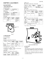
Page 2: ...ified Value Instrument Connection MTT 111 Variable Resistor in motor 3 000 30 Hz Speaker Ter minal Load resistance 6 ohms Figure 1 Test Stage Frequency Frequency Display Setting Adjusting Parts Instrument Connection IF 450 kHz 1 602 kHz L305 1 AM Band Coverage 522 kHz fL L306 1 1 0 1 V 2 AM Tracking 990 kHz 990 kHz L302 3 1 Input IC301 1Pin Output IC301 23Pin 2 Input Input is not connected Output ...

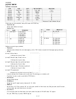
Page 3: ...in unit and then press the POWER button OK appears If only the POWER key is pressed ERROR appears KEY1 KEY2 KEY3 TEST CONTENTS INDICATION Memory Preset Down Power Preset clear Tu CL Memory Stop Power Preset set FM P 01 Memory Play Power Display Memory Preset up Power CD T 1 Memory Clear Power Soft reset CL Bass treble Preset down Power Volume T 3 Bass treble Play Power Timer test T 4 Bass treble C...

Page 4: ...aner disc onto the CD disc tray with the brush side down then press the play button 3 You will hear music for about 20 seconds and the CD player will automatically stop If it continues to turn press the stop button CAUTION The CD lens cleaner should be effective for 30 50 operations however if the brushes become worn out earller then please replace the cleaner disc If the CD cleaner brushes become...

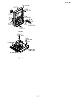
Page 5: ...e disas sembling 4 Take sufficient care on static electricity of integrated circuits and other circuits when servicing STEP REMOVAL PROCEDURE FIGURE 1 Top Cabinet 1 Screw A1 x 5 2 Socket A2 x 2 3 Flat Cable A3 x 1 1 2 Side Panel 1 Screw B1 x 4 1 3 Rear Panel 1 Screw C1 x 2 2 Screw C2 x 2 1 2 4 Main PWB 1 Screw D1 x 2 2 Socket D2 x 2 3 Socket D3 x 1 2 5 Front Panel 1 Screw E1 x 2 3 6 Power PWB 1 Sc...

Page 6: ...Figure 5 Open Cassette Holder G2 x8 ø2 6x10mm H2 x4 ø3x10mm H1 x1 ø2 6x10mm G1 x1 Front Panel Display PWB PWB Spring Lever Tape Mechanism J1 x1 ø2 6x10mm J2 x2 K1 x4 ø2 6x10mm Open Close Switch PWB Top Cabinet CD Mechanism ...

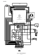
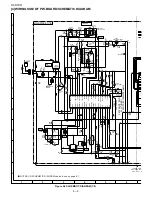
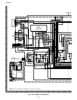
Page 7: ...IN PD AGC AMLOWOUT DET OUT MPX IN VDD XOUT XIN D0 CL DI R OUT L OUT FM IET P CCMP P DET CE VSS P DET FMRF IN VCC1 AM MIX GND1 FM MIX REG AMRF IN AM LOOP ANTENNA M ANTENNA FOCUS TRACKING SPIN SLED DRIVER AM OSC FM RF FM OSC FM FRONT END 1 3 2 4 1 2 3 1 2 3 4 5 7 6 12 10 9 8 11 13 LA4631 POWER AMP AMP_A1_ON R L CD_A1_VCC CD_A1_VCC P ON TP VM MA VCC 1 2 3 POWER TRANSFORMER T315mA L 250V AC POWER SUPP...

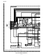
Page 8: ...9 28 27 26 25 24 23 22 21 20 19 18 17 16 15 14 13 12 11 10 9 8 7 6 5 4 3 2 1 F B A E FO TR TR FO ACTUATOR TR FO FO C F B A E 1 2V 5V TR 1 2VCC C D VCC VC LD VR MD D GND GND LD VR MD PD CD PICKUP UNIT SP SP SL SL PU IN GND PICKUP IN SLED MOTOR SPINDLE MOTOR M M 5 1 4 6 2 3 16 15 14 13 12 11 10 9 8 7 6 5 4 3 2 1 CD SERVO FOCUS TRACKING SPIN SLED DRIVER FROM DISPLAY PWB LVDD TP8 1 2 3 1 TAPE MOTOR PL...

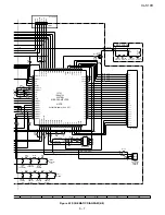
Page 9: ...S2 VDD2 S14 S13 S12 S11 S10 S9 S8 S7 PA7 S6 PA6 S5 PA5 S4 PA4 S3 PA3 S2 PA2 S1 PA1 S0 PA0 P73 INT3 TOIN P72 INT2 P71 AN9 P70 AN8 P87 AN7 P86 AN6 P85 AN5 CF2 P84 AN4 P83 AN3 P82 AN2 P81 AN1 P80 AN0 VDD1 CF1 VSS1 XT2 AN11 XT1 AN10 RESET P17 P16 P15 SC1 P14 SI1 S19 S18 S17 S16 S15 S14 S13 S12 S11 S10 S9 S8 S7 S6 S5 S4 S3 S2 S1 S0 C3 C2 C1 C0 V1 PL4 V2 PL5 V3 PL6 S39 S38 S37 S36 S35 S34 S33 S32 S31 S3...

Page 10: ...8 V 2 23 V 2 25 V 4 0 V 3 9 V 2 9 V 2 43 V 2 43 V 0 V 0 V 0 V 0 V 0 V 0 V 1 82 V 1 67 V 3 9 V 2 24 V 0 69 V 2 57 V 2 1 V 2 5 V 2 0V 3 1 V 2 7 V 2 1 V 4 9 V 5 1 V 4 9 V 5 1 V 0 V 0 97 V 1 2 3 4 5 6 7 8 9 10 11 12 13 14 15 16 17 18 19 20 21 22 23 24 25 26 27 28 29 30 31 32 33 34 35 36 PIN NO VOLTAGE IC301 8 8 V 1 5 V 0 V 1 5 V 1 3 V 11 5 V 17 7 V 0 V 0 V 0 V 0 V 8 4 V 0 V 1 2 3 4 5 6 7 8 9 10 11 12 ...

Page 11: ... 0 022 22 23 24 25 26 27 28 29 30 VP VTCC FM 1 5V 5 0V AM 1V 8V TP VT FMRF IN FMRF OUT VCC2 FM OSC AM OSC B02 B01 LP OUT LP IN PD AGC AMLOWOUT DET OUT MPX IN VDD XOUT XIN D0 CL DI R OUT L OUT FM IET P CCMP P DET CE VSS P DET FMRF IN VCC1 AM MIX GND1 FM MIX REG AMRF IN AM LOOP ANTENNA FM ANTENNA TO MAIN PWB AMP TAPE SEC MAIN PWB A1 1 2 FM RF FM OSC FM BAND COVERAGE fL FM FRONT END NOTES ON SCHEMATI...

Page 12: ... 0 TRK 0 TRK 0 FCS I TRK G FCS 1 FCS GND GND GND 0 FCS GND GND GND MUTE VCCVCC VWRQ VRES DRF CE CL DI DO CONT3 CONT2 PD01 PD02 VVSS PCKIST VVDD VDD5 VSS LDD FR LDS DATA DATACK REF1 TDO ADAVSS ADAVDD JITTC RFMON TE TEC FE RSVSS RFVDD RF VREF TIN2F TIN1E FIN2B FIN1A LCHO LVSS RVSS RCHO RVDD XVDD EFMIN SLCIST SLCO XOUT XIN FSX 16MIN XVSS C2F EFLG IGMOUT ASRACK ASDFIN LRSY TEST DOUT VDD VSS MON15 MON1...

Page 13: ...P GND D GND A GND SP GND P ON TP VM MA VCC GND SD OUT2 BB2 1 2 3 POWER TRANSFORMER T315mA L 250V POWER PWB A3 When Servicing Pay attention as the area enclosed by this line is directly connected with AC main voltage AC POWER SUPPLY CORD AC 230 V 50 Hz HEADPHOMES SPEAKER TERMINAL L CH R CH 2 3 4 5 6 7 1 TO MAIN PWB 1 2 TUNER CD SECTION MAIN PWB A1 2 2 S101 NOT USED 2 1 L R J102 J104 NOTES ON SCHEMA...

Page 14: ...V RECORD PLAYBACK AMP 47P 47P CH CH CH 13 12 11 10 9 8 7 6 5 14 GND SD VCC TRE2 TRE1 VCC2 VOL2 VOL1 SEL OUT1 SEL OUT2 PB2P PB2N PB1P PB1N REC10 REC1N REC2N REC20 C2 C1 B2 B1 A2 A1 OUT1 BB1 OUT2 BB2 R CH L CH RECORD PLAYBACK HEAD ERASE HERD TAPE MECHANISM ASS Y 226 1 8 9 10 11 12 13 14 15 16 17 TO MAIN PWB 1 2 TUNER CD SECTION 550 C506 C507 C513 C511 R506 C516 C515 C521 C524 C535 R561 R563 R562 R56...

Page 15: ...3 3K 3 3K 1 CD LID 2 15P CH CH CH VP D GND O POWER I TP STATE O EVR SCK O EVR SDO O AMP ON O CD CE O CD CLK O CD CMD I CD DATA I CD WRQ O CD RESET 1 CD DRF O TU CE O TU SDO O TU SCK I TU SDI TO MAIN PWB DISPLAY PWB A2 SWITCH PWB A5 ON STAND B TUNING UP 32 768K NOTES ON SCHEMATIC DIAGRAM can be found on page 6 1 R714 R716 R711 R712 R713 R710 R701 R703 R705 R706 R709 R707 R708 R715 R702 R704 CNS701 ...

Page 16: ...A3 S2 PA2 S1 PA1 S0 PA0 P73 INT3 TOIN P72 INT2 P71 AN9 P70 AN8 P87 AN7 P86 AN6 P85 AN5 CF2 P84 AN4 P83 AN3 P82 AN2 P81 AN1 P80 AN0 VDD1 CF1 VSS1 XT2 AN11 XT1 AN10 RESET P17 P16 P15 SC1 P14 SI1 S19 S18 S17 S16 S15 S14 S13 S12 S11 S10 S9 S8 S7 S6 S5 S4 S3 S2 S1 S0 C3 C2 C1 C0 V1 PL4 V2 PL5 V3 PL6 S39 S38 S37 S36 S35 S34 S33 S32 S31 S30 S29 S28 S27 S26 S25 S24 S15 P13 S01 P12 SC0 P11 S10 P10 S00 P07 ...

Page 17: ...3K 3 3K 1 CD LID 2 15P 32 768K CH CH CH VP D GND O POWER I TP STATE O EVR SCK O EVR SDO O AMP ON O CD CE O CD CLK O CD CMD I CD DATA I CD WRQ O CD RESET 1 CD DRF O TU CE O TU SDO O TU SCK I TU SDI TO MAIN PWB 1 2 DISPLAY PWB A2 SWITCH PWB A5 ON STAND B TUNING UP NOTES ON SCHEMATIC DIAGRAM can be found on page 6 1 R714 R716 R711 R712 R713 R710 R701 R703 R705 R706 R709 R707 R708 R715 R702 R704 CNS70...

Page 18: ...A4 S3 PA3 S2 PA2 S1 PA1 S0 PA0 P73 INT3 TOIN P72 INT2 P71 AN9 P70 AN8 P87 AN7 P86 AN6 P85 AN5 CF2 P84 AN4 P83 AN3 P82 AN2 P81 AN1 P80 AN0 VDD1 CF1 VSS1 XT2 AN11 XT1 AN10 RESET P17 P16 P15 SC1 P14 SI1 S19 S18 S17 S16 S15 S14 S13 S12 S11 S10 S9 S8 S7 S6 S5 S4 S3 S2 S1 S0 C3 C2 C1 C0 V1 PL4 V2 PL5 V3 PL6 S39 S38 S37 S36 S35 S34 S33 S32 S31 S30 S29 S28 S27 S26 S25 S24 S15 P13 S01 P12 SC0 P11 S10 P10 S...

Page 19: ...lindrical type without lead wire VC TV Square type without lead wire VC TQ Square type without lead wire VC CY Square type without lead wire VC CZ Square type without lead wire VC J The 13th character represents capacity difference J 5 K 10 M 20 N 30 C 0 25 pF D 0 5 pF Z 80 20 If there are no indications for the electrolytic capacitors error is 20 Resistors VRD Carbon film type VRS Carbon film typ...

Page 20: ...Y1EF473Z J AB 0 047 µF 25V C102 110 VCKYCY1EF104Z J AA 0 1 µF 25V C111 112 RC GZA105AF1H J AB 1 µF 50V Electrolytic 1 C113 114 VCKYCY1EF104Z J AA 0 1 µF 25V C115 116 RC GZV108AF1C J AD 1000 µF 16V Electrolytic C117 RC GZA226AF1H J AB 22 µF 50V Electrolytic C118 RC GZW688AF1E J AH 6800 µF 25V Electrolytic C119 RC GZA107AF1C J AB 100 µF 16V Electrolytic C120 VCKYCY1EF104Z J AA 0 1 µF 25V C121 RC GZA...

Page 21: ...13 VRS CY1JB332J J AA 3 3 kohms 1 16W R114 VRS CY1JB472J J AA 4 7 kohms 1 16W R115 VRS CY1JB332J J AA 3 3 kohms 1 16W R116 117 VRS CY1JB333J J AA 33 kohms 1 16W R118 VRS CY1JB101J J AA 100 ohm 1 16W R119 VRS CY1JB102J J AA 1 kohm 1 16W R120 121 VRS CY1JB822J J AA 8 2 kohms 1 16W R131 132 VRS CY1JB682J J AA 6 8 kohms 1 16W R302 VRD ST2CD100J J AA 10 ohm 1 6W R303 VRD ST2CD104J J AA 100 kohm 1 6W R3...

Page 22: ...splay 232 LHLDZA002SJSA J AD Holder LED 233 LHLDZA003SJSA J AC Lever Record 3 R711 VRD ST2CD102J J AA 1 kohm 1 6W R712 713 VRD ST2CD332J J AA 3 3 kohms 1 6W R714 716 VRS CY1JB332J J AA 3 3 kohms 1 16W R717 VRS CY1JB472J J AA 4 7 kohms 1 16W R718 VRD ST2CD104J J AA 100 kohm 1 6W R719 VRS CY1JB122J J AA 1 2 kohms 1 16W R720 VRD ST2CD122J J AA 1 2 kohms 1 6W R721 VRS CY1JB102J J AA 1 kohm 1 16W R723 ...

Page 23: ...AD Screw ø2 5 10mm 606 XJBSD30P08000 J AA Screw ø3 8mm 607 XJBSD30P10000 J AA Screw ø3 10mm 608 XJBSF25P08000 J AA Screw ø2 5 8mm 609 XJBSF30P12000 J AA Screw ø3 12mm SPEAKER BOX PARTS B3CPXLS10H J BB Speaker Box Ass y L CH R CH ACCESSORIES PACKING PARTS 1 QANTL0004SJZZ J AG AM FM Loop Antenna 2 RRMCGA001SJSA J AP Remote Control GCOVAA003SJSA J AG Battery Lid Remote Control 3 SPAKAA003SJZZ J AE Pa...

Reviews: