(2) AC input section (filter, etc.)
The input filter is of LC filter in one-step composition, and reduces
common mode noises and normal mode noises from the AC line. The
across-the-line capacitor, the line bypass capacitor, and the common
mode choke coil are provided on the AC PWB. the line bypass
capacitors (C805, C806) and across-the-line capacitor C807 (100V
series only) are provided on the power PWB.
The fuse (F802) in the AC line protects the circuit against an abnor-
mal current caused by blow-off or melt-down in the circuit.
(3) Rectifying and smoothing
This section converts the AC power into DC outputs (instable state).
Rectifying and smoothing are made by diode bridge DB801, cement
resistor R822, and smoothing capacitor C814.
Cement resistor R822 limits a rush current caused by charging of
smoothing capacitor C814 when the AC power is turned on.
(4) Main switching circuit section
The instable DC output is turned ON/OFF by the FET transistor in the
hybrid IC (IC802) with the transformer T801 as the load. During the
ON period of the FET transistor, energy is charged in transformer
T801. During OFF period of the FET transistor, energy is discharged
to the secondary side of transistor T801.
C809 is a resonance capacitor which makes LC resonance of the
inductance in the primary winding of transformer T801 and capacitor
C809. When the drain voltage of the FET transistor approaches near
0V, the FET transistor is turned on to reduce power loss.
To take timing to turn on the FET transistor, delay of time constant of
resistors R815 and R812 and capacitors C813 and C812 is used.
(5) Hybrid IC (IC802) pin functions
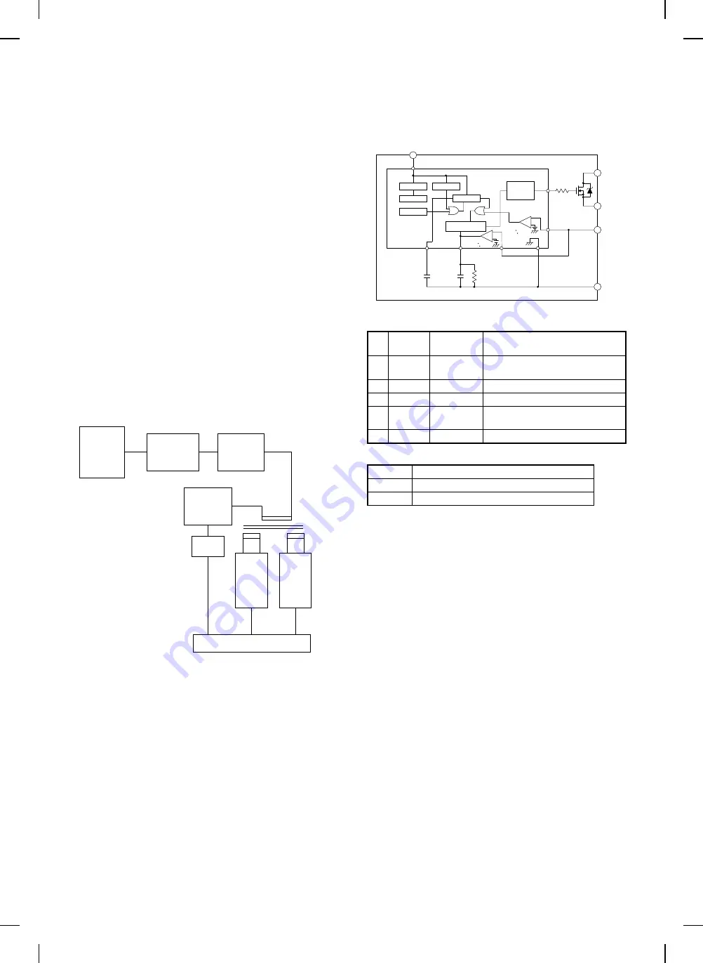
The figure below shows the block diagram of hybrid IC (IC802).
STR-F6515 block diagram
Pin functions
Pin
No.
Code
Name
Function
1
OCP/F.B.
OCP and
feedback pin
Protection of an overcurrent and
constant-voltage control signal input
2
S
Source pin
MOS FET source
3
D
Drain pin
MOS FET drain
4
VIN
VIN pin
Power voltage of the control circuit
grounding
5
GND
GND pin
GND
Other functions
Code
Function
OVP
Built in the overvoltage protection circuit.
TSD
Built in the overheating protection circuit.
1) VIN pin (No. 4 pin), start circuit
The start circuit detects the VIN pin voltage to start or stop the
operation of hybrid IC (IC802).
When the AC power is turned on, capacitor C808 is charged
through starting resistors R810 and R811. When the VIN pin volt-
age reaches 16V (TYP), the control circuit stops the operation.
After the control circuit is actuated, the voltage of auxiliary winding
of transformer T801 is rectified and smoothed to provide the
power.
2) OCP/FB pin (No. 1 pin), oscillator, constant-voltage control circuit
The oscillator utilizes charging and discharging of C1 built in the
hybrid IC (IC802) and capacitor C812, generating pulse signals to
turn ON/OFF the FET transistor. The constant-voltage control is
performed by determining the OFF time of the FET transistor by
the delay time determined by the time constant of resistors R815
and R812 and capacitors C813 and C812. The ON time control
varies the pulse width of the oscillator directly.
The OCP/FB pin voltage is biased by the current of photo coupler
PC801 so that the detected voltage of shunt regulator IC801 on
the secondary side of the power is constant. As a result, the ON
time of the FET transistor is controlled to stabilize the VB output.
The voltage drop of R816 and R817 connected between the FET
transistor source pin (2 pin) and the GND pin (5 pin) to detect the
drain current of the FET transistor. The threshold voltage of over-
current detection is about 0.75V (TYP).
Connector
harness
CN802
803
AC filer
F802
Rectifying
/smoothing
Main switch
control
IC802
ON/OFF
circuit
Rectifying
/smoothing
Rectifying
/smoothing
F801
SWEN
ON/OFF
signal
VBS
+14V
non-stabilizing
line
VB
+24V line
Connector CN801
Start
4
Vin
Reg.
T.S.D
O.V.P
Latch
O.S.C
Comp.2
=1.35V
C2
C1
R1
+
-
Drive
R2
3
D
2
S
1
O.C.P/F.B.
5
GND
Comp.1
=0.75V
+
-
12 – 13
www.freeservicemanuals.info
1/11/16
Published in Heiloo, Holland.


