background image

PC-UM10M

SL-5500   DIAGNOSTICS AND CHECK ITEMS

– 50 –

CHAPTER 5. DIAGNOSTICS AND CHECK ITEMS

When diag are executed, data of user will be cleard.
If you need the data, you must transfer the data before starting diag.

1. DIAG MENU

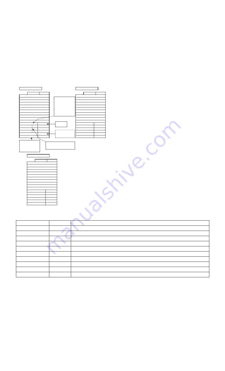
Entering the DIAG mode: Press and hold [P] and [D] keys, and press FULL RESET button simultaneously.

Key operations

When the Normal Diag Mode (Diag Menu (3/3) No. 10) is executed, if “Full reset” is made, the diag is booted.

To boot the OS, execute Clear Diag Flag (Diag Menu (3/3) No.4).

DIAG MENU (2/3)

Page down

Page up

1. Idle mode
2. 16pin
3. SD Card
4. Low Battery
5. RAM
6. Compact Flash
7. Flash (SUM)
8. Sounder
9. Remocon
10. Charge

AIN1(B/U)
AIN1(Main)
AIN0
Tablet
COM

Version

M.B.L

SD WP

SD CD

CF  CD

:

:H

:H

:H

:X

:

:

:

:X

DIAG MENU (1/3)

Page down

Page up

1. COM ADJ setting
2. AGING
3. Battery Voltage Adjust
4. Touch Panel
5. LCD+LED
6. IrDA
7. Main Keyboard
8. Slide Keyboard
9. Earphone
10. Front Light

AIN1(B/U)

Boot Flag       : 

Boot Flag       : 

AIN1(Main)
AIN0
Tablet
COM

Version

M.B.L

SD WP

SD CD

CF  CD

V           :

V           :

:

:H

:H

:H

:X

:

:

:

:X

AIN1 (B/U): Backup  battery voltage
AIN1 (Main): Main  battery voltage
AIN0: Battery pac k presence/absence

When a value is set, the
display is as follows:
   Tablet: 0
   COM: Set value
If there is no set value: X

Indicates status  of 
battery voltage  or battery
replacement SW.

Indicate the 
ROM Version

  When the machine is
reset while "Boot Flag:Diag"
is displayed, the Diag booted.

DIAG MENU (3/3)

Page down

Page up

1. Irda Checker
2. 

4. Clear Diag Flag
5. 
6. 
7. CF Update
8. 
9. 
10. Normal Diag Mode

Tablet
COM

Version

M.B.L

SD WP

SD CD

CF  CD

:

:H

:H

:H

:X

:

:

:

:X

AIN1(B/U)
AIN1(Main)
AIN0

  When the machine is
reset while "Boot Flag:"
is displayed, the OS booted.

---

---

---

Boot Flag       : 

V           :

---

Slide key

Main key

Operation

Cancel (on/off)

Turns on the power.

Cursor upper

A

Shifts the selected menu item upward.

Effective only on the menu display.

Cursor lower

D

Shifts the selected menu item downward. 

Effective only on the menu display.

Cursor right

B

Refer to the next page 

Effective only on the menu display.

Cursor left

L

Refer to the previous page. 

Effective only on the menu display.

OK

ENTER

Starts the selected check

Cursor key center

1

Interrupts the check under process and returns to the menu.

C OK

Fn + ENTER

Writes the set value while the common voltage is being adjusted. 

Front Light

Turns on/off the Front Light. (Toggle operation)

1,2,.....9,0

Selects and execute the menu. 

Effective only on the menu display.

Summary of Contents for Zaurus SL-5500

Page 1: ...document has been published to be used for after sales service only The contents are subject to change without once CODE 00ZSL5500SM E Personal Mobile Tool MODEL SL 5500 CHAPTER 1 SPECIFICATIONS 1 CHAPTER 2 HARDWARE DESCRIPTION 4 CHAPTER 3 DISASSEMBLY AND ASSEMBLY 31 CHAPTER 4 NOTES FOR SERVICING 47 CHAPTER 5 DIAGNOSTICS AND CHECK ITEMS 50 CHAPTER 6 TROUBLE SHOOTING 60 CHAPTER 7 CIRCUIT DIAGRAM PA...

Page 2: ... Reflective TFT LCD with Front light Touch sensitive panel supported 3 5 with 240 x 320 pixels 65 536 colors Memory ROM 16MB FLASH for OS Applications Driver etc RAM 64MB SDRAM Input Device Touch panel Type writer keyboard Character Input QWERTY Keyboard with a slide cover Software keyboard hand writing Pick board similar to cellular phone input Internet Mail POP3 IMAP4 SMTP File attachment capabi...

Page 3: ... inserted after the rechargeable back up battery is fully charged approx 5 minutes Number of charging and discharg ing of the operating battery life Approx 500 times Note The Battery life and storage time may vary depending on the usage Power Consumption 2 5 W with battery 6 2 W with AC adapter Temperature Range For operation 0 C to 40 C 32 F to 104 F For charging battery 5 C to 35 C 37 F to 99 F ...

Page 4: ...t key Display Cursor key OK key EMail key Menu Popup key Front light key HOME key Address Book key Display Protection cover Eyelets for the Handstrap Battery Compartment Lid FULL RESET button Battery Replacement Switch Stylus CF Card Slot CF Slot Protection Card Stereo Headphone Jack IR port SD card slot Connection Terminal inside SYNC button SHARP I O PORT AC Adapter Jack USB Cable ...

Page 5: ...z Osc PLL 32kHz Osc Interrupt controller Powe Management Reset controller GPIO10 13 RS 232 USB Func EXPAND connecter 16pin Serial1 UART Serial4 MCP SSP Serial0 USB Serial3 UART Serial2 IRDA ARM SA 1 core I cache 16k byte D cache 8k byte mini cache Peripheral Bridge LCDC DMA Memory PCMCIA control JTAG Misc Test SA1110 Strong_ARM 256pin BGA DAC M62332 AUDIO DAC VR LCD timing control 72pin QFP CS4 PW...

Page 6: ...35143_RESET MIC_ON nREMOCON_1k_ON STEREO_64FS CO 9 21MHz CF_DETECT TC35143_IRQ WAKEUP 16pin GA_INT MainBatt LOW 32kOUT GPIO0 GPIO1 GPIO2 GPIO3 GPIO4 GPIO5 GPIO6 GPIO7 GPIO8 GPIO9 GPIO10 GPIO11 GPIO12 GPIO13 GPIO14 GPIO15 RTS CTS DTR DSR LCD_VSHA_ON LCD_VSHD_ON LCD_VEE_ON LCD_MOD DAC_ON F L_VR DAC_SDATA DAC_SCK DAC_SLOAD nSD_DETECT nSD_WP SD_VCC_ON GA LOCOMO GPIO0 GPIO1 GPIO2 GPIO3 GPIO4 GPIO5 GPIO...

Page 7: ... the details of the system design 3 SYSTEM CONFIGURATION 3 1 BLOCK DIAGRAM 3 2 SA 1110 FUNCTIONAL DIAGRAM OSC 3 686 MHz OSC 32 768 KHz PLL1 PLL2 RTC OS Timer General Purpose I O Interrupt Controller Power Management Reset Controller JTAG and Misc Test IMMU DMMU Dcache 8 Kbytes Minicache Write Buffer ARM SA 1 Core Memory and PCMCIA Control Module Bridge DMA Controller Serial Channel 0 UDC Icache 8 ...

Page 8: ...OCZ SDRAM RAS This signal should be connected to the row address strobe RAS pins for all banks of SDRAM nSDCAS OCZ SDRAM CAS This signal should be connected to the column address strobe CAS pins for all banks of SDRAM SDCKE 1 0 OCZ SDRAM and or SMROM clock enables SDCKE 0 should be connected to the clock enable CKE pins of SMROM SDCKE 0 is asserted upon any rest including sleep exit if static memo...

Page 9: ... General purpose input output SMROM_EN IC Synchronous mask ROM SMROM enable This pin is used to determine if the boot ROM static memory bank 0 is asynchronous or synchronous If asynchronous boot ROM is selected SMROM_EN 0 and its width is determined by the state of the ROM_SEL pin SMROM is supported only on 32 bit data bus ses ROM_SEL IC ROM select This pin is used to configure the ROM width It is...

Page 10: ...ckage 3 SYSTEM BLOCK DIAGRAM nRESET_OUT OCZ Reset out This signal is asserted when nRESET is asserted and deasserts when the processor has com pleted resetting nRESET_OUT is also asserted for soft reset events sleep and watchdog nTRST IC Test interface reset Note this pin has an internal pull down resistor and must be driven high to enable the JTAG circuitry If left unconnected this pin is pulled ...

Page 11: ... factors output from the control resistor to this terminal are set The signal level at the time of interrupt is active high RST 55 D I HOST System reset This signal is active low TSPX 45 A I O HZ IN TSC Interface terminal for touch screen X plate Open when not in use TSMX 43 A I O HZ IN TSC Interface terminal for touch screen X place Open when not in use TSPY 42 A I O HZ IN TSC Interface terminal ...

Page 12: ...a default state Pull down when not in use GPIO1 50 D I O HZ IN GPIO GPIO GPIO2 51 D I O HZ IN GPIO GPIO GPIO3 52 D I O HZ IN GPIO GPIO GPIO4 62 D I O HZ IN GPIO GPIO GPIO5 63 D I O HZ IN GPIO GPIO GPIO6 1 D I O HZ IN GPIO GPIO GPIO7 2 D I O HZ IN GPIO GPIO GPIO8 3 D I O HZ IN GPIO GPIO GPIO9 4 D I O HZ IN GPIO GPIO TEST1 7 D I ETC Test pin Fix to GND TEST2 6 D I ETC Test pin Fix to GND VREF 25 A I...

Page 13: ...block Low power consumption Parameter block configuration TELOP Relay ON OFF TELON SCLK SSYNC SDIN SDOUT TELIP TELIN VBO1P VBO1N VBI1P VBI1N VBI2P VBI2N IRQ RST TEST1 TEST2 TSPY TSPX TSMY TSMX VBO2P VBO2N DVDD1 to DVDD2 DVSS1 to DVSS2 AIN0 AIN1 AIN2 AIN3 AVDD1 to AVDD2 AVSS1 to AVSS2 CVSS1 to CVSS2 VREF GPIO 9 0 TC35143AF Hand set Microphone Speaker Digital power supply Digital grand Analog power ...

Page 14: ...e enable This pin controls writing to CUI and memory array The address and data are latched at the leading edge of CE or WE whichever comes first WP Input Write protect When WP is VIL The release of lock bit in the block to which lock down bit is set is prohibited For blocks to which either lock bit or lock down bit is not set erasure or program operation can be performed Lock down bit can be disa...

Page 15: ... and DUTY can be changed Fixed output at PWREN and internal Enbit Inverted output at INVbit is possible When BATTFAULT pin input level is Low the register of this module is initialized 2 3 2 Block diagram 2 4 LED CONTROLLER 2 4 1 Outline This module outputs the pulse modulation output signal for LED light emission to the LEDPWM0 1 pins It has the following features Outputs the pulse modulation out...

Page 16: ...is module are initialized when batterfault pin input level is LOW The operation of this module does not depend upon pwren pin input level 2 10 2 Block diagram Here is a circuit image LRCEN SCEN LRCINV LRCEVE LRCRST SCINV TiAudio Format Standard Data Format Initialize sclk pin sfrm pin CPU bus lrclk Reset lrclk Leading and trailing sclk Inversion Register settings dacsck output pin lrclk output pin...

Page 17: ...k64fs 88 O sda 87 O scl 86 O lrclk 85 O dacsck 84 vdd3 83 O xout24m 82 I xin24m 81 gnd 80 I adr2 79 I adr3 78 I adr4 77 I adr5 76 I adr6 75 I adr7 74 I adr23 73 I adr24 72 I adr25 71 vdd3 70 I ki15_b 69 I ki14_b 68 I ki13_b 67 I ki12_b 66 I ki11_b 65 I ki10_b 128 O adstart 127 I oe_b 126 I we_b 125 I cs_b 124 gnd 123 I reset_b 122 I test 121 O int_b 120 I pwren 119 I rtc32k 118 I battfault 117 I c...

Page 18: ...B 15 0 16 IN IBH Key input signal external pull up resistance is required KEY_BOARD Subtotal 24 Serial output circuit for general purpose 8 bit 2ch DAC control SCL 1 OUT OD1T Serial clock signal DAC SDA 1 IN OUT BG1 Serial data DAC Subtotal 2 TFT_C reset TFTRESET 1 OUT OB1T TFT_C reset signal TFT PS control CPS 1 OUT OB1T TFT power save CPS output signal TFT panel AD_START output circuit for table...

Page 19: ...I O BA1T General purpose I O port CMOS input Feed through current prevention type GPIO 14 13 2 1 4 I O BH1T General purpose I O port Schmidt input TEST circuit TEST 1 IN ITST1 Test mode selection signal input Power supply 3 3 V VDD3 7 GND 8 TOTAL_PIN 128 QFP15 14 x 14 x 1 4mm Function Pin name Pin No Q ty I O Buffer Description Connected to IBC Input buffer IBH Schmidt trigger input buffer IBO OR ...

Page 20: ...n I 26 ENAB Horizontal display position signal input pin I 27 VDD Power supply input pin 28 GND Grounding power supply pin 29 RESET Initialization reset signal input pin Give the sig nal which changes L level to H level and holds it when power is turned on I 30 REV Common electrode generation signal output pin O 31 REVV0 Base voltage generation signal output pin O 32 PS Source driver control signa...

Page 21: ...C Non connection pin Release electrically 69 TV SPS output timing setting pin I 70 TESTI Test input pin Usually set to H I 71 HS Horizontal synchronous signal input pin Positive polarity input I 72 VS Vertical synchronous signal input pin Positive polarity input Pin No Signal name Description I O REV REV PS 3DCLK CLS LP SPL SPR OR0 OR5 OG0 OG5 OB0 OB5 CLK R0 R5 G0 G5 B0 B5 ENAB DCLK HS Tc 0 4Tc 0 ...

Page 22: ... to L Display 240H Display 240H RESET INTPCCARD IC401 VACT CVCCDOWN CVCC3EN CVCC5EN CVPP3EN CVPP5EN CCD1 CCD2 BVD1 STSCH BVD2 SPKR CRESET CVS1 CVS2 INTC CS4 WE OE nPIOIS16 nPWAIT nPIOR nPIOW nPWE nPOE nPCE 1 2 nPREG A 25 0 PSKTSEL GPIO GPIO D 15 0 Intel StrongArm SA 1110 LVDD 3 3V Always ON HVDD 5 3 0V CF PCMCIA D 15 0 RDY BSY A 25 0 REG CD 1 2 OE WE IOR IOW WAIT WP IOIS16 Inside REG Power supply ...

Page 23: ...5 PA7 LVDD 3I PA8 3I PA9 3I PA10 3I S 40 PA11 3I S PA12 3I S 38 PA13 GND GND 74 CD3 5IO 75 CD4 5IO CD11 5IO CD5 5IO CD12 5IO CD6 5IO 80 HVDD CD13 5IO CD7 5IO CD14 5IO CCE1_B 5O 85 CD15 5IO CA10 5O CCE2_B 5O COE_B 5O CA11 5O 90 GND CIORD_B 5O CA9 5O CIOWR_B 5O CA8 5O 95 CA17 5O CA13 5O CA18 5O CA14 5O CA19 5O 100 HVDD CWE_B 5O CA20 5O CRDY 5I CA21 5O CA16 5O CA22 5O 107 CA15 5O GND PA14 3I S Buffer...

Page 24: ...ti level Delta Slgma Modulator Zero Detect Power Supply Output Amp and Low pass Filter DAC DAC Output Amp and Low pass Filter VOUTL VCOM VOUTR ZEROL ZEROR VDD DGND VCC AGND PIN NAME TYPE DESCRIPTIONS 1 BCK IN Audio data bit clock input 1 2 DATA IN Audio data digital input 1 3 LRCK IN L channel and R channel Audio data latch enable input 4 DGND Digital ground 5 VDD Digital power supply 3 3V 6 VCC A...

Page 25: ...uring short load peaks and compatibility with Li ion batteries is guaranteed by an accurate current limiting function 2 BLOCK DIAGRAM 3 PIN CONFIGURATION 4 PINNING P type POWER FET TEMPERATURE PROTECTION START UP CIRCUIT LX ILIM GND SYNC SHDWN FB UPOUT DNIN U D 4 2 6 5 8 1 7 3 N type POWER FET I V CONVERTER I V CONVERTER 13 MHz SYNC GATE OSCILLATOR TIME COUNTER DIGITAL CONTROLLER BAND GAP REFERENC...

Page 26: ...ground for 0 5A peak inductor current limit TTL input threshold 10 9 8 7 6 2 1 3 4 5 PVIN VIN I LIM BLON SHDN FB LX GND PGND VOUT 10 Pin MSOP SP 6650 5 SHDN Shutdown control input Tie to VIN for normal oper ation tie to ground for shutdown TTL input thresh old 6 FB External feedback network input connection Con nect a resistor from FB to ground and FB to VOUT to control the output voltage external...

Page 27: ...ESET O LOW 17 Reserve MIC_ON O Microphone input enable at L LOW 18 UART_SCLK1 in nREMOCON_1k_ON O Enable at LOW HI 19 SSP_CLK in STEREO_64FS_CLK I 20 UART_SCLK3 in CO I Charging at LOW of the charging indicator 21 MCP_CLK in 9 21MHz I from GA TC35143 Synchroniza tion clock SIBCLK 22 TREQA MBREQ in CF_DETECT I from_CF_GA 23 TREQB in TC35143_IRQ I from TC35143AF 24 Reserve WAKEUP 16pin I from 16pin ...

Page 28: ...ed off IO_4 AMP_ON O ON at HI The power is turned off IO_5 Board version I SL5000 L SL5500 L The power is turned off IO_6 Sounder bias O ON at HI The power is turned off IO_7 MAIN_BATT_SW_ON O ON at HI The power is turned off IO_8 B U_BATT_SW_ON O ON at HI The power is turned off IO_9 TEMP_ON O ON at HI The power is turned off LOCOMO GPIO0 RTS O LOW 1 CTS I 2 DSR I 3 DTR O LOW 4 LCD_VSHA_ON O ON a...

Page 29: ...SCOOP PA11 CHRG_ON O H output when charg ing Status hold PA12 For booting Diag I Enabled only when reset start INPUT PA13 For booting Diag I Enabled only when reset start INPUT PA14 MUTE_L O Earphone mute control Mute at L LOW PA15 MUTR_R O Earphone mute control Mute at L LOW PA16 5V_ON O Diag ON at H OFF at L PA17 AMP_CN2 O ON at HI LOW PA18 VPEN_CN2 O WP cancel at HI Lock down bit an be changed ...

Page 30: ...ev B4 ROMP capacity x32 bus fixed nCS0 3 16MB nCS1 3 Not Use nCS2 3 Not Use nCS3 3 Not Use PC slot A 3 CF NCS4 3 GA CF_GA NCS5 3 Not Use RAM capacity SDRAM nMCS0 3 64MB nMCS1 3 Not Use nMCS 3 Not Use Optical communication IrDA1 2 115kbps Sharp GP2W0110YP USB slave only USB1 1 16 pin connector Touch panel Resistance sheet type LCD HR TFT 320 x 240 dots SD card Yes CF card Type ΙΙ F L brightness con...

Page 31: ...falls below 3V Adapter 5 V DC DC 3 3 V DC DC 3 3 V DC DC VDT 3 0 V Reg 3 1 V VDT 3 3 V VDT B U Batt MAIN Batt 2 0 V 1 8 V DC DC SW 4 SW 3 SW 2 SW 1 VCC Core VCC 5 VCC 3 AC_Adaptor Battery 950mAh Discharge max 2 3A Fatal 3 6V about 5V DC DC Step_up 3 3V DC DC Step_Down 1 8V DC DC Step_Down CPU SDRAM Mask_ROM Flash_ROM Inverter 300mA Regurater TK11133 Regurater TK11133 IR_Unit TC35143AF DAC PCM1741 ...

Page 32: ...ure to confirm the click Sound when inserting the Stylus completely 2 Remove and insert the Stylus 2 or 3 times to check that insertion is made smoothly c Display Protection Cover Installation 1 Apply grease to the Display Protection Cover Rib and wipe with cloth 2 Check that the Display and Upper Cabinet sections around the display are free from scratches dirt and dust 3 Engage the Display Protec...

Page 33: ... groove between the LCD Main PWB unit and the Lower Cabinet and open and disengage the lock pawl in the arrow direction 3 Put your fingers in the clearance between the upper cabinet and the LCD Main PWB unit and slowly lift and remove the upper cabinet in the arrow direction A 4 Remove the LCD Main PWB unit from the Lower Cabinet In the arrow section the stereo headphone jack equipped in the main ...

Page 34: ...e Out Ribbon and attach the Duplex Tape of the other half of the ribbon to the outside of the Battery Stor age section 5 Press the attachment section to assure attachment 2 Assembly of the Battery Replacement Switch and the IR Filter and the Nut Cushion 1 Attach the Battery Replacement Switch 2 to the Lower Cabinet 1 2 When attaching the Lower Cabinet be sure to set the Battery Replacement Switch ...

Page 35: ... Cabinet Unit 1 Check that the following parts are attached to the Lower Cabi net Unit A IR Filter Battery Replacement Switch I O Cover I O Holder Battery Take Out Ribbon Nut Cushion 2 First insert the Stereo Headphone Jack of the Lower Cabinet Unit A then engage the Pawls 3 Be careful not to pinch the lead wire white of the Cool CRT If it should be pinched check that the coating of the lead wire ...

Page 36: ...f the Slide Cover Fixture into the sliding groove 4 Hold the sides of the Slide Cover Unit 1 and slide it back and forth 3 times to apply grease evenly Check at the same time that it slides smoothly 5 Open the Slide Cover Unit 1 fully and check that the contact spring is not deformed when viewed from the set sides and the I O Port 6 When assembling be careful not to scratch the Upper Cabinet and d...

Page 37: ...fter insertion do not twist it or do not apply a load to it It would cause disconnection of the connector Tighten the screws in the sequence of 1 to 2 When tightening the screws do not apply an excessive force No Part name 1 LCD Unit 2 Main PWB Unit 3 Inverter Holder 4 Inverter Fixing Tape 5 Inverter Unit 6 Sub PWB Unit 7 Screw D 8 Stylus Holder 9 Boss Cap 6 7 5 4 9 9 3 2 1 8 1 Sub PWB Unit disass...

Page 38: ...d 1 When processing the lead wire of the Cool CRT be careful not to damage the coating cover Never use a sharp cutter for processing of the lead wire Never use the Cool CRT with damaged or broken coating cover of lead wire Never use an inverter unit that was dropped or damaged by a strong shock 2 Since the PWB of the Inverter Unit 5 is fragile be sure to hold the connectors when connecting the lea...

Page 39: ... connector 3 3 Check the connection state 4 When locking use an anti static electricity holder to prevent the PWB from being deflected 5 Be careful to prevent breakage of Lock Pawl of the connector 6 Bend the FPC of the LCD Unit 5 and cover it over the PWB 7 Hang the LCD Holder 6 Pawl on the PWB Unit 2 and fix it 8 Pass the Tablet Pin 1 through the slit of the PWB 9 Release locking of the connecto...

Page 40: ...e below Right and left sides Check that the Slide Cover is fixed to the cabinet rib at two posi tions 3 Screw A x 4 tightening Be careful not to apply an excessive force No Part name 1 Slide Cover Cabinet 2 Key Top A1 Cancel 3 Key Top A2 OK 4 Key Top A3 HOME 5 Key Top B Cursor 6 Key Top C Center 7 Slide Cover Fixture 8 Screw A 9 Screw B F Slide Cover Lock G Key PWB Unit H Key Rubber B I Key PWB Sh...

Page 41: ...y installed 2 When taking reversing the Key Rubber B be careful not to drop the Key Top 3 Be careful to prevent the Key Rubber Key Top from covering the cabinet ribs and key holes Key Top A1 Key Top A3 Key Top A2 Attach the projection to the lower side Key Top B Key Top C Fit the Key Top B rib with the groove Be careful to the direction Use the notch in the brim of Key Top B and the groove in the ...

Page 42: ...ith IPA from the Fixing Tape Attachment section of the Slide Cover Panel 2 Separate the Slide Cover Panel Fixing Tape from the Mount Sheet 3 Attach the Slide Cover Panel Fixing Tape to the Slide Cover Panel Note Attach the tape so that it does not cover the rib Note Be careful that the sheet must not cover the cabinet pawl and screws Corner attachment reference Corner attachment reference Corner a...

Page 43: ... to ensure attachment 2 Fixing Key Panel attachment Clean and remove oil with IPA from the attachment section of the Fixed Key Panel of the Upper Cabinet Attach the Key Panel with out extending over the cabinet 3 LED Indicators x 2 attachment Insert the LED Indicators x 2 from the front surface of the Upper Cabinet Note 1 When pressing and fixing the Slide Cover Panel do not touch the Key PWB cont...

Page 44: ...I O Holder 5 NOTE FOR THE MAIN PWB UNIT PARTS LIST 0 5 0 0 0 5 Attachment reference Attachment reference Fixing Tape I O Holder I O Cover I O Holder Grease application area Apply grease also to the same area on the other side No Part name 1 Main PWB Move Unit 2 CF Card Connector Frame 3 Battery Section Insulation Sheet 4 PWB Insulation Sheet 5 AC Adapter Jack 6 Stereo Headphone Jack 7 Contact Spri...

Page 45: ...awls 2 pcs Either the front or the back may be soldered Attach and fold the CF Tape to the CF Card Connector Frame according to the reference below Note 1 The sheet must not extend out of the outward form of the PWB 2 There must be free from wrinkles folds and projec tions by pinching foreign materials 3 There must be free from dirt and fingerprints If there is remove completely 0 0 2 Attachment r...

Page 46: ...1 BR503 BR504 BR601 BR602 BR603 BR604 BR707 BR803 BR806 BR807 BR902 BR905 C101 C1011 C1012 C102 C103 C104 C105 C106 C107 C108 C109 C110 C111 C112 C117 C118 C119 C120 C121 C202 C203 IC613 C206 C207 C209 C301 C345 C350 C351 C352 C353 C354 C355 C356 C404 C409 C502 C503 C505 C506 C507 C508 C509 C510 C511 C512 C513 C517 C518 C608 C609 C610 C611 C612 C614 C615 C616 C632 C633 C634 C635 C636 C637 C638 C64...

Page 47: ...is not attached the battery will be heated to smoke Use great care to avoid it The Back Up Battery Insulation Sheet must not extend out of the external shape of the sub PWB 3 Back Up Battery Cushion attachment Attach the Back Up Battery Cushion according to the attachment reference shown below The Back Up Battery Insulation Sheet must not extend out of the external shape of the sub PWB No Part nam...

Page 48: ... or sharp tip 4 Replace the Battery Compartment Lid Note Be sure to replace the Battery Compartment Lid before you use 5 Slide the Battery Replacement Switch to the NORMAL OPERA TION position 6 Press Cancel On Off to turn the power ON The Welcome screen appears Then follow the next procedures to complete the initial settings Adjusting the touch panel Setting the date and time Registering your pers...

Page 49: ...ied by Sharp PC Windows 95 98 NT4 0 2000 Parallel terminal for bi directional communication SL 5500 1 Install the Flash Memory Write Program into the PC Install the program into the JTAG write PC referring to Readme txt in the program supplied by Sharp The Readme txt may contain the latest information which is not covered in this document 2 Remove the Main Battery and AC Adapter from the SL 5500 A...

Page 50: ...S OF THE LATEST SOFTWARE Install the latest software after completion of repair as follows 1 Prepare PC card type CF card adapter with CF FROM card 64MB 2 Download the latest updated software file zip file from the web site http developer sharpsec com 3 Unzip the zip file on PC OSPACK file will be created 4 Copy the file to the root directory of the CF card 5 Insert the CF card to the SL 5500 6 Co...

Page 51: ... presence absence When a value is set the display is as follows Tablet 0 COM Set value If there is no set value X Indicates status of battery voltage or battery replacement SW Indicate the ROM Version When the machine is reset while Boot Flag Diag is displayed the Diag booted DIAG MENU 3 3 Page down Page up 1 Irda Checker 2 4 Clear Diag Flag 5 6 7 CF Update 8 9 10 Normal Diag Mode Tablet COM Versi...

Page 52: ... Press OK key White background u u MIN White background is displayed F L turns on 5 Press OK key Gradation u u 2nd Black on the lower side and white gradually increases as it goes up 6 Press OK key Black white one point check pattern u u 3rd Check pattern F L is rather bright 7 Press OK key Black white one point check pattern u u MAX Check pattern F L is rather bright 8 Press OK key Black backgrou...

Page 53: ... 1 3 3 Touch the Page up Select No 1 Idle mode of DIAG MENU 2 3 Idle mode ON current A1 160mA or less 4 Press F L key of the SL 5500 DIAG MENU 1 3 F L ON F L current A1 550mA or less 5 Press on off key once to turn off the power turn off OFF current A1 1mA 2 75mA 6 Supply power of 3 2V to the backup battery side V2 3 2V V1 0V SW1 OFF SW3 OFF B U current A2 1mA 2 5mA CP601 GND Main GND A1 V1 SL 550...

Page 54: ...HECK DIAG MENU 1 3 Page down Page up 7 Main Keyboard 8 Slide Keyboard AIN1 B U Boot Flag AIN1 Main AIN0 Tablet COM Version M B L SD WP SD CD CF CD V H H H No Operating procedure Display Check item 1 Connect the AC adapter to supply power to the SL 5500 and press FULL RESET button to boot the DIAG menu DIAG MENU 1 3 2 Select No 8 Slide Keyboard Press Activity key 3 Shift the slide key down Press Ac...

Page 55: ...s FULL RESET button to boot the DIAG mode If the DIAG is not booted by pressing FULL RESET button press and hold P D and press FULL RESET button simultaneously 2 Press Front Light key to turn on the light DIAG MENU 1 3 Front Light turns on 4 Press OK key 5 Check for the set value which provides no flicker of display with the cursor key There is no flicker of display 6 Remember the adjustment value...

Page 56: ...3 3 Select No 4 Touch Panel Touch Panel Menu 3 Touch Calibration 4 Scribble 4 Press OK key Select Touch Calibration Touch panel adjustment screen 6 Touch two marks for 1sec or more At that time the value is written into the Flash ROM White background The marks are changed to red 7 8 Press on off key and press cursor center key DIAG MENU 1 3 9 Press on off key After the display is turned off comple...

Page 57: ...H No Operating procedure Display Check item 1 In DIAG MENU 1 3 touch Version at the right lower section of the display Version List CPU SA1110 B4 or SA1110B5 Board 01 ROM USA Version ROM C S Check sum 2 Press the center key of the cursor to return to the menu DIAG MENU 1 3 3 Press on off key to turn off the power After the display is turned off completely remove the Main battery Test target SL5500...

Page 58: ...ed normally it is OK For operating procedures refer to the Operation Manual SL5500 Use Docking Station CE ST7 SL5000 Use Docking Station CE ST6 1 Open DIAG MENU 1 3 2 Connect a stereo headphone or a speaker with amplifier to the stereo headphone jack Do not put the stereo headphone in the ears because it produces too big sounds 3 Tap No 9 Earphone Operation Display Test content 1 Check the dis pla...

Page 59: ...DSR H 3 Make RTS L Check that CTS H Make DTR H Check that WAKEUP L Note Supply this IC power from VCC GND of 16in connector Check that DSR L ic 74HC14 or 74HC04 4 Make RTS H Check that CTS L Make DTR H Check that WAKEUP H Check that DSR L 14 pin DTR 7 pin DSR 5 pin RTS 6 pin CTS 10 pin WAKEUP Test jig CE 170TS PC with RS 232 9pin support The terminal adapter confirmed by Technical Division is Tera...

Page 60: ... MENU 2 3 2 Install the AC Adapter EA 70 and the SYCARD CFtest220 3 Tap No 6 Compact Flash Display CF Connector Check Status messages Test procedure 0 CD1 CD2 1 Data 15 8 REG WE RD 2 Data7 0 CE1 IOWR IORD WAIT 3 AddressBus A10 A0 CE1 CE2 OE 4 VCC BVD1 BVD2 WP RDY 5 VS1 VS2 At last if the display indicates as below it is OK Status messages ...

Page 61: ...user data should be recovered back up the user data before executing the diag operations 1 Check the operation with the user s battery pack Check the battery replacement switch Press the ON OFF key 2 Enter the diag mode and press any key Does operate Return to the user Explain that the power is not turned on with the battery replacement switch at REPLACE Does not operate Connect the AC adapter and...

Page 62: ...indicated on AIN0 and AIN1 on the lower side of the diag menu 2 Does X903 oscillate X903 18 432 MHz 3 Is FPC of the tablet disconnected Is it properly connected to the connector No display Check soldering of IC501 IC901 Connect the adapter and enter the diag mode No main battery DIAG MENU 1 4 Select 3 Battery Voltage Adjust Select No 1 Battery Voltage Adj DIAG MENU 2 4 Select 10 Charge Select ON I...

Page 63: ...nector terminal of each card 1 Check CF CD and SD CD on the right lower side of the diag menu 2 Insert the CF card and the SD card and check again 3 When the CF card is inserted no operation is performed All should be H All should be L NG Remains at H The card is not recognized When the CF card is not recognized When the SD card is not recognized Check CD pin of the connector and check CCD of BR40...

Page 64: ... O PORT CF I O PORT I O PORT I O PORT 1 2 C104 47U 4V A 1 2 C108 10U 10V A PSKTSEL PSKTSEL TP131 PAD TP132 PAD TP133 PAD 2 1 R128 47k 1005 J TP135 PAD TP123 PAD TP129 PAD TP130 PAD UART_TXD UART_TXD RXD_C B1 TXD_C C2 VDDX2 E12 VSSX A1 VDD C1 VSS D3 D0 E4 D8 D2 D16 D1 D24 E3 D1 F4 D9 E2 D17 E1 D25 F3 VDDX2 F12 VSSX B2 D2 F2 D10 F1 D18 G4 D26 G3 D3 G2 D11 H6 D19 G1 D27 H4 VDD H3 VSS H2 VDDX2 G5 D4 H...

Page 65: ...C9 DQ10 D1 DQ9 D2 VDDQ D3 VSSQ D7 DQ6 D8 DQ5 D9 DQ8 E1 NC E2 VDD E7 LDQM E8 DQ7 E9 UDQM F1 CLK F2 CKE F3 CAS F7 RAS F8 WE F9 VSS E3 A12 G1 A11 G2 A9 G3 BA0 G7 BA1 G8 CS G9 A8 H1 A7 H2 A0 H7 A1 H8 A10 H9 VSS J1 A5 J2 A4 J3 A3 J7 A2 J8 VDD J9 A6 H3 IC201 K4S561633C RL75 SA_D16 SA_D17 SA_D18 SA_D19 SA_D20 SA_D21 SA_D22 SA_D23 SA_D24 SA_D25 SA_D26 SA_D27 SA_D28 SA_D29 SA_D30 SA_D31 SA_A20 SA_A10 SA_A1...

Page 66: ...PR REVV0 REV TFTRESET L_BIAS L_PCLK L_FCLK VSHD SPS CLS SPS CLS R 0 4 B 0 4 G 0 5 R 0 4 G 0 5 B 0 4 R0 R1 R2 R3 R4 G0 G1 G2 G3 G4 G5 B0 B1 B2 B3 B4 P S 34 DGND 33 VSHD 32 B5 31 B4 30 B3 29 B1 27 V1 41 V0 40 VSHA 39 SPR 38 LBR 37 DCLK 36 LP 35 V8 48 V7 47 V6 46 V5 45 V4 44 V3 43 V2 42 V9 49 AGND 50 B2 28 VEE 10 VEE 9 VSS 8 CLS 7 SPS 6 U L 5 MOD 3 R3 17 R2 16 R1 15 R0 14 SPL 13 VCOM 12 VCOM 11 G4 24...

Page 67: ...U 10V 1608 2 1 C409 1U 10V 1608 AMP_ON2 AMP_ON2 PSKTSEL CF_IRQ CF_DETECT nSA_WE nSA_CS4 nSA_OE nSA_PIOW nSA_PWE nSA_POE nSA_PIOR nSA_PWAIT nSA_PCE2 nSA_PREG nSA_IOIS16 nSA_PCE1 nRESET_IN PSKTSEL CF_IRQ CF_DETECT nSA_WE nSA_OE nSA_CS4 nSA_PIOW nSA_PWE nSA_PIOR nSA_POE nSA_PWAIT nSA_PCE2 nSA_PREG nSA_IOIS16 nSA_PCE1 nRESET_IN TP402 TP401 TP404 TP403 TP406 TP405 TP408 TP407 TP410 TP409 TP412 TP411 TP...

Page 68: ..._DOUT CLK9M SIB_DIN TC35143_IRQ AIN0 AIN1 AIN3 CPU Q501 POWER POWER I O PORT REMOCON 1 2 C503 10U 10V A NO FUSE 1 2 C510 10U 10V A NO FUSE 1 2 C511 10U 10V A NO FUSE 1 2 C512 10U 10V A NO FUSE 2 1 R511 22 1005 J 2 1 C516 open 1005 TP502 TP501 TP504 TP503 TP506 TP505 TP508 TP507 1 BR504 BR2 470k 1005 2 1 R516 0 1005 J 2 1 R515 OPEN 1005 J 2 1 R514 0 1005 J 2 1 R513 OPEN 1005 J 2 1 C517 1u 10v 1608 ...

Page 69: ...3 EVOUTA 4 VCNTA 5 VCNTB 6 V 7 GND 8 VREF 9 REFIN 10 EVROUT 11 EVOUTB 12 OP INB 13 OP INB 14 IC604 NJM2172 AVCC3 AGND2 2 1 C656 OPEN 1608 2 1 R641 OPEN 1005 2 1 R642 OPEN 1005 K A D602 OPEN 1SS355 AGND2 AGND2 AGND2 AVCC3 1 2 C653 10U 10V A NO FUSE 2 1 R652 220 1005 J AGND2 1 2 3 4 5 6 D2 S1 D1 G1 S2 G2 Q605 FDC6303N MUTE L MUTE R AUDIO L ch AUDIO R ch Vdd 5 IN 3 Vss 2 IN 1 Out 4 IC611 TC75S51FU 2 ...

Page 70: ... N140 N139 K A D802 DSP10G K A D824 DSP10G 2 1 C832 1UF 10V 1608 F 2 1 F809 200mA 1608 13 N293 N301 N292 N283 N259 N282 N281 N280 N279 N278 2 1 R852 130K 1608 D 2 1 R853 43K 1608 D 2 1 R851 300K 1608 D 2 1 R855 470 1608 F 2 1 C836 1UF 10V 1608 F 2 1 L801 D63CB 4 7u K A D826 RB081 20 2 1 C838 47PF 50V 1005 2 1 L802 D63CB 22u 2 1 C840 1UF 10V 1608 F 2 1 C844 1UF 6 3V 1005 2 1 F810 0 1608 2 1 F811 0 ...

Page 71: ...19 IC301 IC301 IC601 IC601 2 1 R908 10K 1005 J D S G Q901 2SK3019 1 BR906 BR2 1K 1005 5 1 BR902 BR4 470K 1005 2 1 R909 0 1005 2 1 R910 open 1005 HS_OUT HS_OUT 3 2 1 X901 CSTCW 22 5792MHz 3 2 1 X902 CSTCW 24 576MHz 3 2 1 X903 CSTCV 18 432MHz IC401 1 BR907 BR2 470K 1005 SD_VCC_ON SD_VCC_ON ROMSEL ROMSEL TP901 GND 1 XIN18M 2 XOUT18M 3 VDD3 4 DCLK 5 CPS 7 TFTRESET 8 CLK9M 9 DATA3 14 DATA4 15 DATA5 16 ...

Page 72: ... KSTRB0_B KSTRB1_B 5 1 BR703 4 22K 1005 5 1 BR705 4 22K 1005 TC35143_VCC Y1199YC KEY connect pattern VCC3 nRESET_IN CPU TC35143 GPIO3 CPU IR_DIN CPU IR_DOUT GA GA GA GA GA GA GA GA KSTRB3_B KSTRB3_B KSTRB6_B KSTRB5_B KSTRB4_B KSTRB3_B KI5_B KI6_B KI7_B KI8_B KI9_B KI10_B KI11_B KI12_B KI13_B KI14_B 5 1 BR706 4 1K 1005 KSTRB 3 6 _B VCC3 VCC3 MAIN_BATT_LOW MAIN_BATT_LOW 2 1 C705 0 1UF 16V 1005 1 2 C...

Page 73: ...S2 TXD0 RXD0 SCK2 SCK0 1 1 3 3 4 4 2 2 5 5 6 6 8 8 9 9 7 7 10 10 11 11 13 13 14 14 12 12 15 15 16 16 18 18 19 19 17 17 20 20 CN1001 DF17 2 020DP 0 5V 2 1 F1001 0 1608 SOUNDER SOUNDER BT1001 BATTERY ML 2012 1SELL TP1011 TP1013 TP1016 TP1007 N16 TP1015 TP1014 TP1012 TP1017 TP1019 TP1005 TP1006 TP1008 TP1009 TP1002 TP1001 TP1003 D S G Q1002 2SK3019 1 2 C1010 10u 10V A 2 1 R1015 0 1005 J K A D1005 MA2...

Page 74: ... LUMII SW LS15A2 T S1 S2 D1 D2 KS38 LUMII SW LS15A2 T S1 S2 D1 D2 KS39 LUMII SW LS15A2 T S1 S2 D1 D2 KS47 LUMII SW LS15A2 T S1 S2 D1 D2 KS48 LUMII SW LS15A2 T KI2 B KI1 B KI0 B KSTRB0 B KSTRB1 B KSTRB2 B KSTRB3 B KSTRB4 B ACTIVITY CONTACT NOME MAIL MENU O K POWER 1 2 3 4 CN1001 Connect Pattern 1 2 3 4 CN1002 Connect Pattern S1 S2 D1 D2 KS29 LUMII SW LS15A2 T CENTER A B C D 8 7 6 5 4 3 2 1 1 2 3 4 ...

Page 75: ...C815 IC813 IC811 L604 L605 L606 L607 L608 LED801 LED901 Q1003 Q1004 Q501 Q601 Q602 Q605 Q608 Q801 Q802 Q804 Q830 Q815 Q902 R1007 R1008 R1009 R1010 R1013 R1014 R103 R104 R105 R108 R109 R110 R111 R112 R113 R114 R115 R125 R126 R127 R128 R130 R133 R135 R201 R202 R203 R303 R310 R318 R319 R325 R328 R330 R403 R404 R405 R502 R503 R504 R505 R506 R507 R508 R509 R511 R517 R607 R601 R602 R603 R605 R606 C210 R...

Page 76: ... D603 D801 D802 D804 D805 L802 D824 F301 F302 F601 F801 F803 F809 IC301 IC305 IC309 IC604 IC801 IC807 IC901 IR701 L301 L601 L602 L801 L803 L804 Q301 Q302 Q303 Q304 R204 Q805 Q810 Q901 R131 R132 R134 R136 R301 R302 R304 R305 R306 R307 R308 R309 R311 R312 R313 R314 R315 R316 R317 R321 R322 R327 R401 R402 R622 R623 R624 R625 R637 R649 R651 R652 R655 R657 R659 R702 R703 R801 R806 R809 R814 R819 R823 R...

Page 77: ...19 KS27 KS18 KS38 KS17 KS08 KS09 KS37 KS29 KS39 KS47 KS48 SP D1005 Q1004 C1013 R1017 R1015 R1016 CN1001 R1006 CN1002 C1006 R1002 R1004 R1005 Q1002 R1012 R1011 F1001 IC1002 C1008 IC1003 C1009 L1001 D1002 C1003 D1003 IC1001 C1005 R1003 R1019 R1020 R1018 C1014 D1006 C1010 ...

Page 78: ... 42 41 36 35 37 36 37 40 38 38 39 SLIDE COVER UNIT 50 49 48 47 46 45 44 MAIN PWB UNIT SUB PWB UNIT 51 52 53 8 9 11 10 UPPER CABINET UNIT 13 14 12 18 16 17 15 LOWER CABINET UNIT 22 21 20 23 24 25 26 27 LCD PWB UNIT 1 1 1 1 1 1 3 4 5 6 7 DOCKING STATION 57 2 19 1 ...

Page 79: ...ertor holder 25 D U N T K 2 2 4 7 Y C Z Z CE N E Main PWB unit include No 44 50 26 L H L D Z 1 0 6 2 Y C Z Z AD C Stylus holder 27 D U N T L 2 2 6 2 Y C Z Z CA E LCD unit 28 P T P E H 1 1 0 2 Y C Z Z AC D Slideing sheet A 29 L X B Z 1 2 3 9 C C 0 1 AB C Screw B 30 P S H E Z 1 1 0 1 Y C Z Z AH C Key PWB sliding sheet 31 D U N T K 2 2 4 9 Y C S 2 AR N E Key PWB unit 32 P G U M M 1 0 3 0 Y C Z 1 AL C...

Page 80: ...witch SW731 SW732 SW733 SW734 SW735 Q S W K 0 2 3 7 A F Z Z AC B Tact switch SW736 SW737 SW738 SW739 SW740 Q S W K 0 2 3 7 A F Z Z AC B Tact switch SW741 SW742 SW743 SW744 SW745 Q S W K 0 2 3 7 A F Z Z AC B Tact switch SW749 SW750 SW754 SW755 SW755A Q S W K 0 2 3 7 A F Z Z AC B Tact switch SW756 SW757 SW758 12 Q S W P 1 0 1 2 P C Z Z AE B Push switch SPVC21 4p SW759 13 Q S W P 1 0 6 3 Y C Z Z AD B...

Page 81: ...C K Y C Z 1 C F 1 0 4 Z AB C Capacitor 16WV 0 10µF C801 C803 C902 C903 C841 C904 59 V C K Y C Z 1 E B 4 7 2 K AA C Capacitor 25WV 4700p 1005 C647 60 V C K Y C Z 1 E F 2 2 3 Z AA C Capacitor 0 022µF 50V 1005 C505 C506 C507 C508 61 V C K Y C Z 1 H B 1 0 2 K AA C Capacitor 50WV 1000pF C661 C343 62 V C K Y T Q 1 A F 1 0 6 Z AD C Capacitor 10µF 10V GRM42 6F106Z10PT C810 63 V C K Y T Q 1 E B 1 0 5 K AD ...

Page 82: ...16 R131 R132 R134 V R S C Z 1 J B 1 0 5 J AD C Resistor 1 16W 1MΩ 5 1005 R136 R302 R327 R902 R904 R905 128 V R S C Z 1 J B 1 5 2 J AA C Resistor 1 16W 1 5KΩ 5 1005 R607 129 V R S C Z 1 J B 1 5 3 J AD C Resistor 1 16W 15KΩ 5 1005 R317 130 V R S C Z 1 J B 2 0 2 J AD C Resistor 1 16W 2KΩ 5 1005 R650 R645 131 V R S C Z 1 J B 2 2 0 J AA C Resistor 1 16W 22Ω 5 1005 R511 R314 R315 132 V R S C Z 1 J B 2 2...

Page 83: ...Diode MA2ZD02 D1005 D1006 D1003 10 V H D R B 5 2 0 S 3 0 1 AC B Diode RB520S D1002 11 V H I M M 3 0 0 5 F N 1 AF B IC MM3005FNRE IC1003 12 V H I S 8 0 9 2 0 A N M P AF B IC S80920ANMP IC1002 13 V H I T K 1 1 1 3 3 C 1 AE B IC TK11133CS IC1001 14 V R S C Y 1 J D 0 0 0 J AA C Resistor 1 16W 0Ω 5 Jumper 1608Type F1001 R1006 15 V R S C Y 1 J D 1 0 4 J AA C Resistor 1 16W 100KΩ 5 R1020 16 V R S C Z 1 J...

Page 84: ...n Japan t COPYRIGHT 2002 BY SHARP CORPORATION All rights reserved Printed in Japan No part of this publication may be reproduced stored in a retrieval system or transmitted In any form or by any means electronic mechanical photocopying recording or otherwise without prior written permission of the publisher ...

Reviews: