6
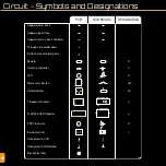
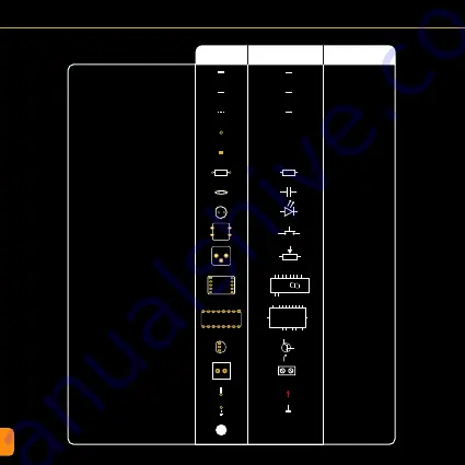
Circuit - Symbols and Designations
Copper power trace
Through hole solder pads
R
C
D
SW
RV
U
U
Q
Copper signal trace
Copper trace on back of board
Surface mount solder pads
Resistor
Ceramic capacitor
LED
Momentary Switch
Potentiometer
7-Segment Display
74HC595 Shift Register
PNP Transistor
Mechanical hole
J
Screw terminal
Connected to GND plane
GND
Connected to VCC
+5V
PCB
SCHEMATIC
DESIGNATION
A
B
C
D
E
F
G
DP
7
6
4
2
1
9
10
5
3
8
CC
CC
3
2
1
QA
QB
QC
QD
QE
QF
QG
QH
Q
H’
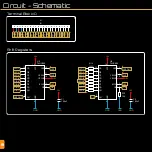
SER
SR
CLK
SR
CLR
RCLK
OE
VCC
GND
3
1
2


