background image

Summary of Contents for SA 400 minifloppy

Page 1: ...SA400 W minifloppyTM Dis ette StorageDrive D 2 I I shUgart Associates ...

Page 2: ...SA400 rt J minifloppyTM Disl etteStorageDrive D 2 2 2 I I Copyright 1977 Shugart Associates ...

Page 3: ...e manual is divided into 3 sections Section I Theory of Operations Section 2 Maintenance Manual Section 3 Illustrated Parts Catalog Each section contains its own Table of Contents For information on the SA 400 drive specifica tions interfacing track formats and applications notes refer to Shugart Associates OEM manual PIN 54102 ...

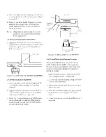
Page 4: ...Section 1 ...

Page 5: ...2 0 Drive Motor Control 6 3 0 Drive Selection 7 3 1 Head Load 7 3 2 Singlle Drive System 7 3 3 Mu Itiple Drive System 7 4 0 Index Detector 8 5 0 Track Zero Indication 9 6 0 Track Accessing 10 6 1 Stepper Motor 10 6 2 Stepper Control 10 6 3 Step Out 10 6 4 Step In Mode 10 7 0 Read Write Operations 13 8 0 Read Write Head 16 9 0 Write Circuit Operation 17 10 0 Read Circuit Operation 18 11 0 Write Pro...

Page 6: ... 13 Track 00 Timing Diagram 9 14 Step Out Logic 10 15 Stepper Control Functional Diagram 11 16 Step Timing Diagram 12 17 Step In Logic 12 1B Bit Cell 14 19 Basic Read Write Head 14 20 Recorded Bit 14 21 Reading A Bit 15 22 IF and 2F Recording Flux and Pu Ise Relationship 15 2 L Read Write Head 16 24 Write Circuit Functional Diagram 17 25 Read Circuit Functional Diagram 18 2B Write Protect Function...

Page 7: ...ead and data may then be recorded or read from the Diskette The drive has two 2 PCB s one is for the drive motor control and the other is the drive PCB The electronics packaged on the drive PCB contains 1 Index Detector Circuits 2 Head Position Actuator Driver 3 Head Load Actuator Driver 4 Read Write Amplifier and Transition Detector 5 Step Control Logic 6 Track Zero Sensing Circuits 7 Write Prote...

Page 8: ...ic surface of the Diskette with minimum Head Diskette wear The SA 400 ceramic head is a single element read write head with straddle erase elements to provide erased areas between data tracks Thus normal tolerance between media and drives will not de grade the signal to noise ratio and insures Diskette interchangeability The read write head is mounted on a carriage which is located on the Head Pos...

Page 9: ...ansferred last Correspondingly the most significant byte of data is transferred to the disc first and the least significant byte is transferred last When data is being read back from the drive bit cell 0 of each byte will be transferred first with bit cell 7 last As with reading the most signifi cant byte will be transferred first from the drive to the user Figure 4 illustrates the relationship of...

Page 10: ... on the using system The SA 400 can use hard sector recording with SAl05 and SAl07 media or soft sectoring using SAl04 media No bits track Bit per inch inside Tracks per inch Access time 1 9 TRACK FORMAT 25 000 bits 2 581 BPI 48 TPI 40 msec loll SOFT SECTOR RECORDING FORMAT In this Format the using system may record one long record or several smaller records Each track is started by a physical ind...

Page 11: ...8 GAP4 J r T GAP BYTES HEX FF SYNC BYTES HEX 00 ID ADDRESS MARK TRACK ADDRESS SECTOR ADDRESS CRC CRC BYTE BYTE 1 2 DATA OR DELETED DATA ADDRESS MARK 128 BYTES OF USER DATA CRC BYTE 1 CRC BYTE 2 I 16 BYTES 4 BYTES j GAP BYTES HEx FF SYNC BYTES HEX 00 WRITE GATE OFF HEX FF GAP BYTES HEX FF SYNC BYTES HEX 00 6BYTES 4BYTES WRITE GATE TURN ON FOR UPDATE OF NEXT DATA FIELD 18YTE 16 BYTES 48YTES t WRITE ...

Page 12: ...art the motor by causing current to flow thm the motor windings Figure 8 shows the functional diagram of the motor speed control cir cuit The motor speed control utilizes an integral brushless tachometer The output voltage signal from this tachometer is compared to a voltage frequency reference level The output from the voltage frequency comparator will control the necessary current to maintain a ...

Page 13: ...e 3 drive select lines In multiple drive sys tems leave the jumper uncut in the shunt block for the drive number you wish to select MX must be cut for the input output to be daisey chained With MX cut drive select must be true in order to activate output enable which in turn gates the out put lines lites the activity lite and conditions the input lines Reading and writing can now be per formed if ...

Page 14: ...to be a valid signal The detector output is fed into a schmidt trigger with a level trigger latch back to maintain pulse stability while shaping the pulse With output enable true this pulse will be on the interface as a negative going pulse Refer to figures 10 and 11 for logic required and timings Shown is the output from a soft sector Diskette 5 0 INDEX SECTOR L I FIGURE 10 INDEX DETECTOR LOGIC _...

Page 15: ...om this And gate conditions another And gate and its other leg is output enable which is true when the drive is selected in a multiple drive system or on power on in a single drive system These conditions will cause a TRK 00 indication to the interface Reference Figure 12 for the logic required OUTPUT ENABLE q A 0 F I DEBOUNCE H ICKT TKOO TP8 FIGURE 12 TRACK 00 INDICATION DIAGRAM __r __ 11 ____ __...

Page 16: ... drive select and read enable true this provides the conditions which allows the step pulse to clock the clock input to the stepper control shift register As the stepper control shifts from one phase to an other the outputs are fed back to the 2nd pulse gen erator sis When a step pulse causes the stepper counter to go from its on track phase via the clock input the two step sis is fired In approxi...

Page 17: ... 5V A Q A D 0 D A D 8 I C HL 01 8 Q OIFIECTION 10 C REAO ENABLE STEP 41 8 FiGURE 15 STEPPER CONTROL FUNCTION DIAGRAM 11 ...

Page 18: ...ECTION A J B I I C n T 11 D n r I FIGURE 16 STEP TIMING Dlt GRAM INPUT TO SECOND PULSE GENERATOR r A B C D _ L A 0 0 0 1 0 0 0 1 0 0 B 0 1 0 0 0 C H O 0 0 0 1 D 1 D ClK PULSE JUU1 fL STEPPER PHASE FIGURE 17 STEP IN LOGIC 12 ...

Page 19: ...e fringe flux mag netizes the surface in a longitudinal direction See Figure 19 7 3 The drive writes 2 frequencies IF 62 5 KHz and 2F 125 KHz During a write operation a bit is recorded when the flux direction in the ring is reversed by rapidly reversing the current in the coil The fringe flux is reversed in the gap and hence the portion of the flux flowing through the oxide recording surface is re...

Page 20: ...ELL 3 BIT CELL 4 BIT CELL 5 BIT CELL 6 BIT CELL 7 0 1 0 1 0 A 1 __ _ J 1 __ J 1 I C HEX I EPRESENTATION FIGURE 18 BIT CELL CURRENT FRINGE FLUX OXIDE CRECORDING SURFACE 1 MYLAR BASE DISKETTE MOTION FIGURE 19 BASIC READ WRITE HEAD CURRENT RECOFIDED BIT DISKETTE MOTION FIGURE 20 RECORDED BIT 14 ...

Page 21: ...2 __i B_I_T_C_E_L_L_3__ IC D C C D c D 1 _ ft JL J _ l n __ n__ J n __ L J I __ 1 I I I r _ _ t I I I wt F iRi ii I FLUX I I I I I REVERSAL V I I I I I I I I L I I I I _ Il IL n n n n READ SIGNAL READ DATA DISKETTE SURFACE WRITE DATA WRITE DRIVER WRITE DRIVER 2 BINARY EQUIVALENT FIGURE 22 1F AND 2F I ECORDING FLUX AND PULSE RELATIONSHIP 15 ...

Page 22: ...one track is recorded it will not splash over to adjacent tracks 8 3 Each bit written will be directed to alternate read write coils thus causing a change in the di rection of current flow through the read write head This will cause a change in the flux pattern for each bit The current through either of the read write coils will cause the old data to be erased as new data is recorded 8 4 On a read...

Page 23: ...Driver provides write current to the other half of the read write coil 9 4 The removal of Write Gate causes the Turn Off Degauss Delay circuit to slowly reduce write current for 25 microseconds During this time if Write Gate is toggled the Read Write head will be degaused by the decreasing write current At the end of the delay the Center Tap Switch opens and the Erase Current Source is turned off ...

Page 24: ...ed to the amplifier section of the read circuit After the amplification the read signal is fed to a filter where the noise spikes are removed The read signal is then fed to the differential amplifier 10 2 Since a pulse occurs at least once every 8 J1S and when data bits are present once every 4 j1S the frequency of the read data varies The read signal amplitude decreases as the frequency increases...

Page 25: ...ut driver if output enable is active This gives a low level to the interface pin 28 The signal and write protect prevents write gate from turning on write current If the WP trace is cut writing to the diskette is inhibited unless a Write Protect label is installed over the notch Figure 26 shows the logic required 5V 1 jV WRITE PRO i ECT SWITCH TP9 o WRITE GATE WRITE CURRENT SOURCE WRITE PROTECT T ...

Page 26: ...ltage and current requirements 12 3 INIPUT OUTPUT LINES There arc four 4 output lines from the SA 400 The output signals are driven with an open collec tor output stage capable of sinking a maximum of 40 ma at a logical zero level or true state with a maximum voltage of OAV measured at the driver When the line driver is in a logical one or false s tate the driver is off and the collector current i...

Page 27: ... 17 4 DIRECTION SELECT 18 19 0 STEP 20 21 4 WRITE DATA 22 23 4 t WRITE GATE 24 25 0 f _TRACK 00 26 27 f WRITE PROTECT 28 29 t READ DATA 30 J2 5 VDC 4 3 4 X 5 RETURN 12 VDC 1 2 4 r t 12 RETURN TJ77 mn AC GND TWISTED PAIR FRAME GND J FIGURE 28 SA400 INTERFACE CONNECTIONS I MAX 10 FEET I RIBBON OR 9 TWISTED PAIR 7t _ FIGURE 29 II lTERFACE SIGNAL DRIVER RECEIVER 21 ...

Page 28: ......

Page 29: ...nd Carriage Assembly 2 4 4 1 Head Write Head Load Button Removal and Installation 2 4 5 Spindle Hub and Pulley Assembly 2 4 6 Clamp Hub Removal 2 4 7 Hub Frame Assembly Removal 2 4 7 1 Hub Frame Assembly Installation and Adjustment 2 4 8 Vllrite Protect Switch Removal 2 4 9 Index Detector Assembly Removal 2 4 10 Index LED Removal 2 4 11 Track Zero Switch Removal 2 4 12 Head Amplitude Check 2 4 13 ...

Page 30: ...Head Load Button Replacement 3 Hub Frame Adjustment 4 Motor Speed Adjustment 5 Track Zero Position 5 1 Track Zero Switch Adjustment 6 Carriage Limiter Adjustment 7 Carriage Limiter Clearance 8 Index Detector Adjustment 9 SA400 Service Position 10 Index Timing 11 Head Radial AI ignment 12 Head Radial AI ignment 13 Write Protect Switch Adjustment 14 Head Load Bail Adjustment 10 10 10 11 15 19 25 3 4...

Page 31: ...he SA 124 to prevent acci dental writing on the SA 124 or if the Write Protect option is utilized remove the Write Protect tab 2 1 2 Exerciser The exerciser is a 800 exerciser with a special cable set The exerciser PCB can be used in a stand alone mode or it can be built into a test station or used in a tester for Field Service The exerciser will enable the user to make all adjustments and check o...

Page 32: ...ot recoverable 2 2 3 Write Error In an error occurs during a write operation it will be detected on the next revolution by doing a read operation commonly called a write check To 2 orrect the error another write and check opera tion must be done If the write operation is not successful after ten 10 attempts have been made a read operation should be attempted on another track to determine if the me...

Page 33: ...d Gated Step Pulses Motor On Preventative maintenance is not required on the SA 400 minifloppy under normal usage 2 4 REMOVALS AND ADJUSTMENTS 2 4 1 Face Plate Removal and Installation a Open the door b Remove the mounting screw on each side of the faceplate Pull the face plate forward and away from the drive casting c No re adjustment is required after replacement J4 7 9 2 J1 1 2 4 3 12 8 11 13 1...

Page 34: ... guide rod nearest the read write head d Pivot the carriage away from the cam and off of the lower guide rod e To re install reverse the above IMPORTANT Insure that after installing the head cable there is enough slack to allow the carriage to go to track zero 4 f Readjust the carriage limiter if a new carriage is installed Reference section 2 4 16 g Head alignment should not be required but if in...

Page 35: ...Put the hub frame onto drive and lightly tighten mounting screws removed in Step 2 of Removal Procedures b Latch the hub frame closed c Position the hub frame until the hub shaft is centered in its mounting hole in the hub frame Reference figure 3 Now tighten the mounting screws for the hub frame pivot springs d Check that the door latch assembly does not bind in the face plate If binding occurs l...

Page 36: ...ernal on TP 7 Index connect one probe to TP 2 and one to TP 1 on the drive PC B Ground the probes to the PCB add and invert one input Set volts per division to 50mv and time base to 20 M seconds per division 6 e Write the entire track with all one s t The average minimum read back amplitude peak to peak should be 80 millivolts If a new load pad does not bring the amplitude to the minimum level try...

Page 37: ...ld be low 3 Step to track 2 T P 8 should remain high FIGURE 6 CARRIAGE LIMITER ADJUSTMENT 2 4 16 Carriage Limiter Fll V Jl NEW STYLE 0 T STEPPER MOTOR SHAFT 020 005 b Step to track zero leave the drive scIected a Unplug the head cable and remove the PCB from the drive leaving the interface and PCB connector installed c Position the stop until it is tlush with stop post old style or in the slot new...

Page 38: ... Alignment Diskette SA 124 I Start the motor and select the drive d Step the carriage to track 01 e Sync oscilloscope external positive on TP 7 Index Set time base to 50 Ilsec division f Connect one probe to TP 1 and the other TP 2 Ground probes to the PCB Set the inputs to AC add and invert one channel Set vertical deflection to 500 MV division g Observe the timing between the start of the sweep ...

Page 39: ...figure 11 g Loosen the two mounting screws which mount the stepper motor to the drive casting h Rotate the stepper motor to radially move the head in or out If the left lobe is less than 70 of the right turn the stepper motor clockwise as viewed from the stepper motor side of the drive If the right lobe IS less than 70 of the left lobe turn the stepper motor counterclock wise as viewed from the st...

Page 40: ...ergize the head load solenoid b Adjust the down stop screw to obtain 3 16 to 1 4 from the top nat surface of the load bail and the platen Reference figure 14 c Check for a minimal clearance of 020 between the load bail and the load arm This check is made at track zero and track 34 with the door closed and the head loaded 10 FIGURE 14 HEAD LOAD BAIL ADJUSTMENT 2 4 21 RI ad Write Head Cleaning Proce...

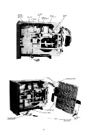
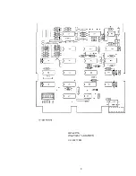
Page 41: ...Physical Locations 11 ...

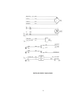
Page 42: ...P4 HEAD CABLE CONNECTOR CLAMP HUB 12 HEAD CABLE EXTENDER ...

Page 43: ...CONNECTOR FRAME GROUND P3 CONNECTOR J1 CONNECTOR J2 CONNECTOR MOTOR __ CONTROL PCB ACTIVITY LIGHT DOOR HANDLE MOTOR PULLEY 13 MOUNTING SCREWS STEPPER MOTOR TACH DISK DRIVE PULLEY ...

Page 44: ......

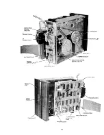
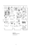
Page 45: ...PCB Component locations 15 ...

Page 46: ... Q1D 20 QD 2 2E i cETIJ 2 F RP4 I I _E C28 r 10000 I I J2 I L DRIVE PCB COMPONENT LOCATIONS Below E C 649 16 ...

Page 47: ...48 C27 C28 I I L J C26 3D lliill 2 3E_1 1R21 R22 R23 R24 Icje0 _f RP4 C J CJ u x IOOO I TEST POINTS DRIIVE PCB COMPONENT LOCATIONS E C 649 TO 692 17 ...

Page 48: ...I L J o o I 2P5 o l 2 D J P4 I 8o o I __nl __ DRIVE PCB COMPONENT LOCATIONS E C 692 AND ABOVE 18 ...

Page 49: ...RED GRN BRN ORG BLU 01 I U CVJ o C J L1AJ G 88 L j R12 J ffi 8ffi II 1 R13 1 R7 I R1 1 C3 ffi 8 COMPONENT LOCATIONS MOTOR CONTROL PCB ASSEMBLY 25063 COMPONENT LOCATIONS MOTOR CONTROL PCB ASSEMB LY PIN 25129 19 ...

Page 50: ......

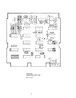
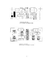
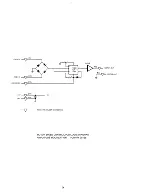
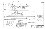
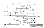
Page 51: ...LogicManual 21 ...

Page 52: ...MX q ______ 0 __ ACTlVITYLED X 16 t t 5V 5V DRVR W DETECT INDEX WRITE GATE 5V J v r DRIVE SELECT 1 INDEX SECTOR DRIVE SELECT 3 VIOTOR ON DR IVE SE LECT 2 OUTPUT ENABLE VVR ITE PROTECT l w D DF1VR 28 Jo X WRITE PROTECT WRITE PROTECT TP 9 NOTES 1 CONNECTOR SYMBOL REFERENCE c J1 W J2 W J3 W J4 2 ALL ODD NUMBERED PINS ON Jl CONNECTOR ARE GROUND GJ PROGRAM SHUNT 3 WITH HM SHORTED HEAD LOADS WITH MOTOR ...

Page 53: ...12V D c B A OUTPUT ENABLE TRK 00 _ _ _ _ _ lD TRACKOO TP 8 5 V 12VA C2 9 0 1 L5 100 12V 10 4 5 6 TP5 10 J rHRU F C27 C14 15 47 21 22 T d T 25 26 l l 01 12V RTN 5V 5V RTN GND GND DRIVE PCB STEPPER CONTIROLS TRACK ZERO POWER 2 OF 2 23 ...

Page 54: ...YEL TACH IN TACH IN MOTOR ON yz_O_R_G_ J BRN 12V v 12V GRD v INDICATES SOLDER CONNECTION DRVR MOTOR OUT BLU MOTOROUT MOTOR SPEED CONTROL PCB LOGIC DIAGRAM AMPLITUDE MODULATION PCB PIN 25129 24 ...

Page 55: ... 12 HEAD LOAD GRY P 3 12V TO SOLENOID WHT PIN L 0HEAD LOAD SOLENOID STEPPER MOTOR YEL COMM GRN V J P 3 II i PIN 6 WHT COMM BRN C P 3 BLK PIN 4 INDEX SECTOR TRACK ZERO N O TRACK ZERO N C WRITE PROTECT GRN L P 3 PIN 8 P 3 PIN J 5V INDEX LED BLU RED INDEX SECTOR LED DET VIO ORG INDEX SECTOR P 3 PIN 5 SWITCH AND MOTOR CONNECTIONS 25 ...

Page 56: ......

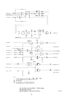
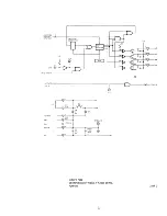
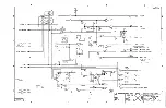
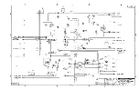
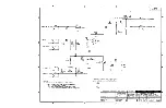
Page 57: ...SCherTlotics 26 ...

Page 58: ......

Page 59: ... B Y 540 I1 OP S J 000 y 5 4 fZ W ZA 0 XS401 1 2 11 0 6 1 I2Z9 12 AJ T 510 X 4o I I TCrfJ I 7 J c rz vJ 1 6 0 B c I I 1 o A EC HISTORY s 1 OI S 6I lo IO J 01 lJ E D MUST CONFORM TO ENGINEERING SPEC ES 30000 0 C O c R 8 L5 Q Z R3G p4 TPI Z MATERIAL TOLERANCE UNLESS DATE NO OTHERWISE NOTED B JG oC OO LINEAR xx P liD OG 1 CASE DEPTH XXX 0 0 8 HARDNESS ANG R 0 111 Z8 SURFACE ES COAlE OUTSIDE MAX 11 0 ...

Page 60: ... 4oo 1 L_ T 3 V II p 13 t ti8 11 J r II STEP 10 rr e CTIOt J 1 le cQ 4 lZV I_ t 1 tG RZ 122 1 2 V 10K 10K 3 12D SV C 1215 C I p NV S I C tl 9 5 4 I 4 _ Cr2 O I IO t l4 10 0 I 2 8_ 2 J 5 L Q A IS 2D 1_ Mr 14D 5 r 9i 3 10 10 C QB 14 V eR li 2 v l5 Q 3 4 BIT L 3C 3C 4 K SREC lQ c 3 1 _ jp A QD R r D QD V 1 CR I 13 3 1 D R I S l I c 13 c12IZ CoRII s ev p 4Ef V l 30 c z 9 2 GTPa R34 3 OO ze Z I E O 4 1...

Page 61: ...tt wRlie PI2 O 540 t 8 _ Nl Tc Pl o TSC T A SHUGRRT l lSSOCIl lTES EC HISTORY MATERIAL TOLERANCE UNLESS DATE NO OTHERWISE NOTED 8 JCo 0b00 UNEAR XX e l o l DETAIL CASE DEPTH XXX 1y 0 18 DESIGN HARDNESS ANGULAR IO ilJ Ol o1 B APPRO 2 SURFACE ES CORNERS OUTSIDE MAX 11 t 0 43 0 PART NO REV EC EDGES 250 1 c TREATMENT ilAOf N INSIDE MAX 11 40 4 MUST CONFORM TO ENGINEERING SPEC ES 30000 0 C31 C 8 L5 Q Z...

Page 62: ... H E T e nn I 12 _ O 1 i j 36 13 J iPl2 12 II r 3E tE f 9 Zf q a 103E S 1 2t C7 SiE P f II CR r V l CQ 14 IZV CTIOIoJ ID I I IO 3 r 1 D R ZS RZ 2 r I A 10 3 2D 5V C RIS 5Y CI l y C1 il 9 I 4 el l0 1 100 0 15 14 10 0 0 I 2 8_ z J 5 L QA 15 1_ M 4D 5 pc IO Q 0 CI QB 14 v el l 3 4 BIT K R El l e I IlolS 3c fiii Z 3 7 _ GP 4 A QD R RG P oo 3D QD r 14E V cPB 1 L cR I 3 v J 1 D R I 0lc C R13 cf21Z eR Sy...

Page 63: ...1 OW1 PUl IJA LE _t_ f 1 540 B D A PART NO REV EC 250 0 4 09C il4 SHUGRRT I lSSOCII lTES EC HISTORY DATE NO 7 78 0940 TOLERANCE UNLESS OTHERWISE NOTED MUST CONFORM TO ENGINEERING SPEC ES 30000 0 MATERIAL HARDNESS ANGULAR 1 I r LINEAR _ x x x 1 IO 7 8T 9 O 4 f1 J i lraI 1 CASE DEPTH C3l Cl2 19 1 5 0 2 f 47 I P5 TP1 2 3 R O T0IC A 1 12A V6 LUE PO T 0 l U U c D n RP Z I 0 y 80n RPI 0 n RP IK I2P4 TYP...

Page 64: ... 4 5 cc i I el I I WRITE t 1 e z4 1 WR 1 O I x 400 I I I DI lE L EoCT O f I t G I I I j be v L 1 I 1 1 2 b 12 I _ nc 2 I I I I 4 I I DR VE E L E T e 4 ill OS B STEP DIRECTlot l B PULL UP I XS400 A 1 SHUGRRT SSOCI TES EC HISTORY DATE NO ES MUST CONFORM TO ENGINEERING SPEC ES 30000 0 MATERIAL SURFACE TREATMENT HARDNESS TOLERANCE UNLESS _ I___O_T HE R W IS E _N_OT_E_D __ _ T r T _T_ l _t LINEAR XJ _ ...

Page 65: ...l 5 D 4 sv DICATGS SOt DE 1 WIRE CONA B TIOA aEF DeSI AlA 101J Re D SIGA AflOAJ LAST SE D NOT t JSE D A REV EC PART NO 250 2 1 1 SHUGRRT r lSSOCII lTES c APPRO SHEET I OF EC HISTORY DATE NO TITLE SCI IGMATIC D A eAM 7 ORV M Ii I SPEED CTI L AM TOLERANCE UNLESS OTHERWISE NOTED ANGULAR MATERIAL 2 HARDNESS SURFACE E_S f RS O UT S ID E __M_A_X _ _ t TREATMENT BROKEN INSIDE MAX CASE DEPTH t LINEAR XX t...

Page 66: ...1 R Pj Vt L 0 12 1 RII a 1 7 10 9 1 1 51 3 4 w 2 2 K 410 1 0 10 Iole 2 W 4 c l U Y6 L w law 1 8 9 2 1K I cl I B L OT I J ED C8 C 25 Q2 RIB NOTEe wtJl E S OTt EIC WI SP5c 1 IED I A LI CA P b CITORS p RE I t 1C ROFt R DS 100 0 2 b LL DIODES A RE IU4148 3 A LL RE SISTORS ARE I OI 4MS 4W 5 lo 4 V Olct iE O 50LOE R E D WI R c oWI 1E C Tlot s UTEqRA T D CIRC Uli I IS TYPE L z 111p j B A A MUST CONFORM T...

Page 67: ...Section 3 ...

Page 68: ...Table f Contents Description Drive Assembly Numeric Index 1 3 4 ...

Page 69: ...ssembly will be level 2 and assemblies within level 2 will have their attaching parts level 3 and so on Parts Replacement Some parts and assemblies are not field replace able These will be noted by an asterisk and a footnote These part numbers are included so they can be ordered for factory and or repair centers Quantity Per Assembly The quantity listed is the quantity used on the assembly Numeric...

Page 70: ... ...

Page 71: ...MOTO R STEPPE R 1 7 SCREW 6 32X 250 BH 2 7 SCFiEW 4AOX 625 BH 2 8 BELT DRIVE 1 8 PULLEY SPINDLE 1 4 BEARING 1 7 SPACER LONG 1 12 SWITCH WR ITE PROTECT 1 2 NUT PLATE 1 6 SCREW 2 56X 50 BH 1 7 LED INDEX 1 5 PLATEN 1 9 SCREW 6 32X 250 BH 1 6 CLAMP PCB 4 11 RETAINER CLAMP 4 7 FACEPLATE 1 0 6 32X 250 F H 2 13 WASHER 1 1 WASHER 1 3 FASTON 1 12 ACTIVITY LIGHT HOLDER 1 15 LED ACTIVITY LIGHT 1 89 GU IDE DI...

Page 72: ... 54 12501 56 15655 32 15663 57 17211 27 17212 45 25060 1 25063 35 54003 24 54006 17 54032 13 54036 51 54038 31 54047 34 54048 41 54055 25 54057 5 54062 46 54064 22 54065 36 54066 9 54067 33 54068 38 54070 2 54073 3 54077 53 54078 15 20 PART NUMBER BEF 54089 60 54090 61 54097 44 54099 18 54125 49 54131 7 54132 8 54135 23 54136 11 54137 48 54138 42 54145 26 4 ...

Page 73: ...22 16 60 ...

Page 74: ...AMP GUIDE ROD 1 26 54145 LOAD BUTTON 1 27 54475 GUIDE DISKETTE RH 1 28 54006 GUIDE ROD 2 29 10186 SCREW 6 32 x 188 BH 4 30 54078 KEEPER GUIDE ROD 1 31 11714 NUT CAPTIVE 2 33 11305 E RING 1 34 10186 SCREW 6 32 x 188 BH 2 35 54073 DOOR HINGE 1 36 54057 STOP DISK 1 37 54132 SPRING CLAMP 1 38 54066 HUB COLLET 1 39 54131 COLLAR HUB 1 40 54032 SPINDLE 1 41 10805 BEARING FLANGED 1 42 54135 BAIL LOAD 1 43...

Page 75: ...63 12 15915 51 17211 20 17212 53 25060 60 25129 11 54003 21 54006 28 54024 62 54030 56 54032 40 54038 17 54040 54 54047 10 54055 22 54056 16 50057 36 7 PART NUMBER REF 54062 52 54064 43 54065 15 54066 38 54068 7 54070 63 54073 35 54077 59 54078 30 54097 2 54125 49 54131 39 54132 37 54135 42 54136 46 54137 47 54138 4 54145 26 54161 5 54473 25 54474 24 54475 27 54479 1 54507 10 54508 9 ...

Page 76: ... ShUgart Associates 435 Oakmead Parkway Sunnyvale Cal ifornia 94086 Telephone 408 733 0100 TWX 910 339 9355 SHUGART SUVL 54096 2 4 79 PRINTED IN U S A ...

Reviews: