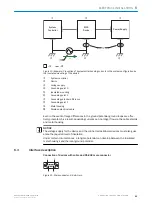
Figure 13: Wiring of a digital input with external NPN sensor
6.4.4
Wiring digital switching outputs
Physical switching outputs on the device
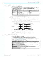
The physical switching outputs can be allocated independently of each other with vari‐
ous functions for event status indication. If the allocated event occurs in the read
process, then the corresponding switching output is live after the end of the clock read‐
ing pulse for the selected pulse duration.
Table 11: Characteristic data for the switching outputs
Switching behavior
NPN switching to supply voltage V
S
Properties
Short-circuit protected
Temperature protected
Not electrically isolated from V
S
Electrical values
The electrical values are identical for all switching outputs.
5 V ≤ V
out
≤ 30 V
I
out
≤ 50 mA
Voltage peak at maximum switching current ≤ 0.8 V
(U
S
−1.5 V) ≤ U
a
≤ U
s
at I
a
≤ 50 mA
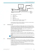
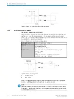
Figure 14: Wiring a switching output
1
Max. load 50 mA
2
DC 5 ... 30 V
Extension: Additional logical switching outputs in the device in the case of physical
“external” switching outputs on the optional connection module
NOTE
Capacitive loads on the switching outputs have an effect on the switch-on and switch-
off behavior. The maximum capacity of 100 mF and an external load resistance of max‐
imum 10 k
Ω
is a limit value.
6
ELECTRICAL INSTALLATION
26
O P E R A T I N G I N S T R U C T I O N S | CLV60x
8021817/10Y9/2018-09-14 | SICK
Subject to change without notice

