Semiconductor Group
3-2
1998-04-01
CPU Timing
C500 Family
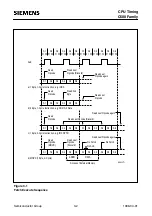
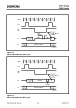
Figure 3-1
Fetch Execute Sequence
ALE
MCD02771
S1
S2
S3
S4
S5
S6
S1
S2
S3
S4
S5
S6
P1 P2
P2
P1
P2
P1
P2
P1
P2
P1
P2
P1
P2
P1
P2
P1
P2
P1
P2
P1
P2
P1
P2
P1
S1
S2
S3
S4
S5
S6
Read
Opcode
Opcode (Discard)
Read next
a) 1 Byte, 1-Cycle Instruction, e.g. INC A
S6
S5
S4
S3
S2
S1
S1
S2
S3
S4
S5
S6
d) MOVX (1 Byte, 2-Cycle)
Read next Opcode (Discard)
S6
S5
S4
S3
S2
S1
S1
S2
S3
S4
S5
S6
Read next
Opcode again
Read 2nd
Byte
Opcode
Read
Read
Opcode
Read next Opcode again
S6
S5
S4
S3
S2
S1
Opcode
Read
(MOVX)
(Discard)
Read next
Opcode
No Fetch
No Fetch
No ALE
Read next
Opcode
Access of External Memory
DATA
ADDR
Read next Opcode again
b) 2 Byte, 1-Cycle Instruction, e.g. ADD A, #Data
c) 1 Byte, 2-Cycle Instruction, e.g. INC DPTR


