background image

Semiconductor Group

4-79

1998-04-01

Instruction Set

C500 Family

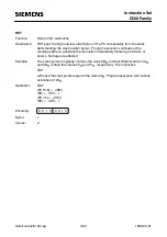
XRL

<dest-byte>, <src-byte>

Function:

Logical Exclusive OR for byte variables

Description:

XRL performs the bitwise logical Exclusive OR operation between the indicated 
variables, storing the results in the destination. No flags are affected (except P, if 
<dest-byte> = A).

The two operands allow six addressing mode combinations. When the destination 
is the accumulator, the source can use register, direct, register-indirect, or 
immediate addressing; when the destination is a direct address, the source can be 
accumulator or immediate data.

Note:

When this instruction is used to modify an output port, the value used as the original 
port data will be read from the output data latch, 

not

 the input pins.

Example:

If the accumulator holds 0C3H (11000011B) and register 0 holds 0AAH 
(10101010B) then the instruction

XRL

A,R0

will leave the accumulator holding the value 69H (01101001B).
When the destination is a directly addressed byte, this instruction can complement 
combinations of bits in any RAM location or hardware register. The pattern of bits 
to be complemented is then determined by a mask byte, either a constant contained 
in the instruction or a variable computed in the accumulator at run-time. The 
instruction

XRL

P1,#00110001B

will complement bits 5, 4, and 0 of output port 1.

XRL

A,Rn

Operation:

XRL2
(A) 

¬

 (A)   (Rn)   

Bytes:

1

Cycles:

1

Encoding:

0  1  1  0

1  r  r  r

v

Summary of Contents for C500

Page 1: ...C500 Microcontroller Family Architecture and Instruction Set UserÕs Manual 04 98 ...

Page 2: ...nsorted or which we are not obliged to accept we shall have to invoice you for any costs in curred Components used in life support devices or systems must be expressly authorized for such purpose Critical components1 of the Semiconductor Group of Siemens AG may only be used in life support devices or systems2 with the express written approval of the Semiconductor Group of Siemens AG 1 A critical c...

Page 3: ...e Datapointers 2 6 2 5 4 Application Example and Performance Analysis 2 6 2 6 Enhanced Hooks Emulation Concept 2 9 2 7 Basic Interrupt Handling 2 10 2 8 Interrupt Response Time 2 12 3 CPU Timing 3 1 3 1 Basic Timing 3 1 3 2 Accessing External Memory 3 3 3 2 1 Accessing External Program Memory 3 3 3 2 2 Accessing External Data Memory 3 4 4 Instruction Set 4 1 4 1 Addressing Modes 4 1 4 2 Introducti...

Page 4: ... and operational characteristics of the SAB 80C52 80C32 the C500 microcontrollers differ in number and complexity of their peripheral units which have been adapted to the specific application areas The goal of this ÒArchitecture and Instruction Set ManualÒ is to summarize the basic architecture and functional characteristics of all members of the C500 microcontroller family This includes the descr...

Page 5: ...ives can use this type of program memory only C500 derivatives with on chip program memory typically use their internal program memory only If the internal program memory is used the EA pin must be put to high level With EA high the microcontroller executes instructions internally unless the address exceeds the upper limit of the internal program memory If the program counter is set to an address ...

Page 6: ...nd after a reset as long as the power supply is not turned off The XRAM content is also maintained when the C500 microcontrollers are in power saving modes 1 2 2 1 Internal Data Memory The internal data memory address space is divided into three basic physically separate and distinct blocks the lower 128 byte of internal data RAM the upper 128 byte of internal data RAM and the 128 byte special fun...

Page 7: ... CD CE CF H C0 C0 C1 C2 C3 C4 C5 C6 C7 H B8 B8 B9 BA BB BC BD BE BF H B0 B0 B1 B2 B3 B4 B5 B6 B7 H A8 A9 A8 AA AC AB AD AE AF H A0 A0 A1 A2 A3 A4 A5 A6 A7 H 98 99 98 9A 9C 9B 9D 9E 9F H 90 90 91 92 93 94 95 96 97 H 88 89 88 8A 8C 8B 8D 8E 8F H 80 80 81 82 83 84 85 86 87 Internal SFR Area direct addressable Byte 128 7FH 7F 7E 7D 7C 3B 7A 79 78 H 30 2FH 70 71 72 73 74 75 76 77 2EH 68 69 6A 6B 6C 6D ...

Page 8: ...nal data memory area called the XRAM This data memory area is logically located at the upper end of the external data memory space except C502 but it is integrated on the chip Because the XRAM is used in the same way as external data memory the same instruction types must be used for accessing the XRAM Figure 1 3 shows a typical 256 byte XRAM address mapping of the C500 microcontrollers Figure 1 3...

Page 9: ...itional 128 byte SFR area called the mapped SFR area The mapped SFR area provides the same addressing capabilities direct addresses bit addressing as the standard SFR area Special Function Register SYSCON Address B1H As long as bit RMAP is set mapped special function registers can be accessed This bit is not cleared by hardware automatically Thus when non mapped mapped registers are to be accessed...

Page 10: ...Port 0 and port 2 are required for accessing external code and data memory and for emulation purposes The external control signals and the clock generation are handled in the external control block The access control unit is responsible for the selection of the on chip memory resources The IRAM provides the internal RAM which includes the general purpose registers The interrupt requests from the p...

Page 11: ...nt and the carry flag it can perform the bit operations of logical AND or logical OR with the result returned to the carry flag The program control section of the core controls the sequence in which the instructions stored in program memory are executed The 16 bit program counter PC holds the address of the next instruction to be executed The conditional branch logic enables internal and external ...

Page 12: ...under software control Bit Function CY Carry Flag Used by arithmetic and conditional branch instruction AC Auxiliary Carry Flag Used by instructions which execute BCD operations F0 General Purpose Flag RS1 RS0 Register Bank select control bits These bits are used to select one of the four register banks OV Overflow Flag Used by arithmetic instruction F1 General Purpose Flag P Parity Flag Always se...

Page 13: ...ry portions Special Function Register DPL Address 82H Reset Value 00H Special Function Register DPH Address 83H Reset Value 00H Special Function Register DPSEL Address D0H Reset Value 00H Bit Function Ð Reserved bits for future use DPSEL 2 0 Data pointer select bits DPSEL 2 0 defines the number of the actual active data pointer DPTR0 7 LSB 1 2 3 4 5 6 7 0 1 2 3 4 5 6 7 LSB MSB Bit No 82H DPL 0 1 2...

Page 14: ... 100 compatibility to the 8051 instruction set This instruction set however allows the handling of only one single 16 bit datapointer DPTR consisting of the two 8 bit SFRs DPH and DPL To meet both of the above requirements speed up external accesses 100 compatibility to 8051 architecture the C500 contains a set of eight 16 bit registers from which the actual datapointer can be selected This means ...

Page 15: ...datapointer then it has to save the old value with two 8 bit instructions and load the new address byte by byte This not only takes more time it also requires additional space in the internal RAM 2 5 4 Application Example and Performance Analysis The following example shall demonstrate the involvement of multiple data pointers in a table transfer from the code memory to external data memory Start ...

Page 16: ... 2 MOV DPL LOW SRC_PTR Load Source Pointer 2 MOV DPH HIGH SRC_PTR 2 INC DPTR Increment and check for end of table execution time CJNE É not relevant for this consideration Ð MOVC A DPTR Fetch source data byte from ROM table 2 MOV LOW SRC_PTR DPL Save source_pointer and 2 MOV HIGH SRC_PTR DPH load destination_pointer 2 MOV DPL LOW DES_PTR 2 MOV DPH HIGH DES_PTR 2 INC DPTR Increment destination_poin...

Page 17: ...MOVC A DPTR Fetch source data byte from ROM table 2 MOV DPSEL 07H Save source_pointer and load destination_pointer 2 MOVX DPTR A Transfer byte to destination address 2 POP DPSEL Save destination pointer and restore old datapointer 2 Total execution time machine cycles 12 The above example shows that utilization of the C500Õs multiple datapointers can make external bus accesses two times as fast as...

Page 18: ... design and reduces costs of an ICE system ICE systems using an EH IC and a compatible C500 are able to emulate all operating modes of the different versions of the C500 This includes emulation of ROM ROM with code rollover and ROMless modes of operation It is also able to operate in single step mode and to read the SFRs after a break Figure 2 3 Basic C500 MCU Enhanced Hooks Concept Configuration ...

Page 19: ...ollowing addresses 0003H 000BH 0013H 001BH 0023H 002BH 0033H 00FBH Figure 2 4 Interrupt Vector Addresses Example of the C501 An interrupt source indicates to the interrupt controller an interrupt condition by setting an interrupt request flag The interrupt request flags are sampled in each machine cycle The sampled flags are polled during the following machine cycle If one of the flags was in a se...

Page 20: ...gram Note that if an interrupt of a higher priority level goes active prior to S5P2 in the machine cycle labeled C3 in figure 2 5 then in accordance with the above rules it will be vectored to during C5 and C6 without any instruction for the lower priority routine to be executed Thus the processor acknowledges an interrupt request by executing a hardware generated LCALL to the appropriate servicin...

Page 21: ...onger response time would be obtained if the request was blocked by one of the three previously listed conditions If an interrupt of equal or higher priority is already in progress the additional wait time obviously depends on the nature of the other interrupt s service routine If the instruction in progress is not in its final cycle the additional wait time cannot be more than 3 cycles since the ...

Page 22: ...cution of a one cycle instruction begins at S1P2 when the opcode is latched into the instruction register If it is a two byte instruction the second reading takes place during S4 of the same machine cycle If it is a one byte instruction there is still a fetch at S4 but the byte read which would be the next op code is ignored discarded fetch and the program counter is not incremented In any case ex...

Page 23: ...1 Cycle Instruction e g INC A S6 S5 S4 S3 S2 S1 S1 S2 S3 S4 S5 S6 d MOVX 1 Byte 2 Cycle Read next Opcode Discard S6 S5 S4 S3 S2 S1 S1 S2 S3 S4 S5 S6 Read next Opcode again Read 2nd Byte Opcode Read Read Opcode Read next Opcode again S6 S5 S4 S3 S2 S1 Opcode Read MOVX Discard Read next Opcode No Fetch No Fetch No ALE Read next Opcode Access of External Memory DATA ADDR Read next Opcode again b 2 By...

Page 24: ...latch The address byte is valid at the negative transition of ALE Then in a write cycle the data byte to be written appears on port 0 just before WR is activated and remains there until WR is deactivated In a read cycle the incoming byte is accepted at port 0 just before the read strobe RD is deactivated During any access to external memory the CPU writes FFH to the port 0 latch the special functi...

Page 25: ... port 2 latch the special function register does not have to contain 1 s and the contents of the port 2 SFR are not modified If the external memory cycle is not immediately followed by another external memory cycle the undisturbed contents of the port 2 SFR will reappear in the next cycle Figure 3 3 and 3 4 show in detail the timings of the external data memory read and write cycles MCD02772 S1 P1...

Page 26: ...2 P1 S2 P2 P1 S3 P2 P1 S4 P2 P1 S5 ALE RD P0 DPL or Ri Out P2 Sampled Data States Float Float PCL out if program memory is external DPH or P2 SFR Out PCH or P2 SFR PCH or P2 SFR MCD02774 S4 P1 P2 P2 P1 S5 P2 P1 S6 P2 P1 S1 P2 P1 S2 P2 P1 S3 P2 P1 S4 P2 P1 S5 ALE WR P0 DPL or Ri Out P2 States PCL out if program memory is external DPH or P2 SFR Out PCH or P2 SFR PCH or P2 SFR Data Out PCL Out ...

Page 27: ...programmed with 8051 assembler or high level languages 4 1 Addressing Modes The C500 uses five addressing modes Ð register Ð direct Ð immediate Ð register indirect Ð base register plus index register indirect Table 4 1 summarizes the memory spaces which may be accessed by each of the addressing modes Register Addressing Register addressing accesses the eight working registers R0 R7 of the selected...

Page 28: ...e address is the sum of a base register DPTR or PC and index register ACC This mode facilitates look up table accesses Boolean Processor The Boolean processor is a bit processor integrated into the C500 family microcontrollers It has its own instruction set accumulator the carry flag bit addressable RAM and l O The bit manipulation instructions allow Ð set bit Ð clear bit Ð complement bit Ð jump i...

Page 29: ...location currently addressed by SP Ð POP transfers a byte operand from the stack location addressed by the SP to the destination operand and then decrements SP Accumulator Specific Transfers Ð XCH exchanges the byte source operand with register A accumulator Ð XCHD exchanges the low order nibble of the source operand byte with the low order nibble of A Ð MOVX performs a byte move between the exter...

Page 30: ... unsigned multiplication of the A register by the B register returning a double byte result A receives the low order byte B receives the high order byte OV is cleared if the top half of the result is zero and is set if it is not zero CY is cleared AC is unaffected Division Ð DIV performs an unsigned division of the A register by the B register it returns the integer quotient to the A register and ...

Page 31: ...s equal to the last bit rotated out SWAP rotates A left four places to exchange bits 3 through 0 with bits 7 through 4 Two Operand Operations Ð ANL performs bitwise logical AND of two operands for both bit and byte operands and returns the result to the location of the first operand Ð ORL performs bitwise logical OR of two source operands for both bit and byte operands and returns the result to th...

Page 32: ... as the offset 0 255 to the address in the DPTR register Thus the effective destination for a jump can be anywhere in the program memory space Conditional Jumps Conditional jumps perform a jump contingent upon a specific condition The destination will be within a 256 byte range centered about the starting address of the next instruction Ð 128 to 127 Ð JZ performs a jump if the accumulator is zero ...

Page 33: ...ng and a symbolic description or restatement of the function is also provided Note Only the carry auxiliary carry and overflow flags are discussed The parity bit is always computed from the actual content of the accumulator Similarly instructions which alter directly addressed registers could affect the other status flags if the instruction is applied to the PSW Status flags can also be modified b...

Page 34: ...on bit 128 software flags any bit addressable l O pin control or status bit A Accumulator Notes on Program Addressing Modes addr16 Destination address for LCALL and LJMP may be anywhere within the 64 Kbyte program memory address space addr11 Destination address for ACALL and AJMP will be within the same 2 Kbyte page of program memory as the first byte of the following instruction rel SJMP and all ...

Page 35: ...r bits of the incremented PC op code bits 7 5 and the second byte of the instruction The subroutine called must therefore start within the same 2K block of program memory as the first byte of the instruction following ACALL No flags are affected Example Initially SP equals 07H The label ÓSUBRTNÓ is at program memory location 0345H After executing the instruction ACALL SUBRTN at location 0123H SP w...

Page 36: ... bit 7 but not out of bit 6 otherwise OV is cleared When adding signed integers OV indicates a negative number produced as the sum of two positive operands or a positive sum from two negative operands Four source operand addressing modes are allowed register direct register indirect or immediate Example The accumulator holds 0C3H 11000011B and register 0 holds 0AAH 10101010B The instruction ADD A ...

Page 37: ...r Group 4 11 1998 04 01 Instruction Set C500 Family ADD A Ri Operation ADD A A Ri Bytes 1 Cycles 1 ADD A data Operation ADD A A data Bytes 2 Cycles 1 Encoding 0 0 1 0 0 1 1 i Encoding 0 0 1 0 0 1 0 0 immediate data ...

Page 38: ...a carry out of bit 7 but not out of bit 6 otherwise OV is cleared When adding signed integers OV indicates a negative number produced as the sum of two positive operands or a positive sum from two negative operands Four source operand addressing modes are allowed register direct register indirect or immediate Example The accumulator holds 0C3H 11000011B and register 0 holds 0AAH 10101010B with the...

Page 39: ...oup 4 13 1998 04 01 Instruction Set C500 Family ADDC A Ri Operation ADDC A A C Ri Bytes 1 Cycles 1 ADDC A data Operation ADDC A A C data Bytes 2 Cycles 1 Encoding 0 0 1 1 0 1 1 i Encoding 0 0 1 1 0 1 0 0 immediate data ...

Page 40: ...enting the PC twice op code bits 7 5 and the second byte of the instruction The destination must therefore be within the same 2K block of program memory as the first byte of the instruction following AJMP Example The label ÓJMPADRÓ is at program memory location 0123H The instruction AJMP JMPADR is at location 0345H and will load the PC with 0123H Operation AJM P PC PC 2 PC10 0 page address Bytes 2...

Page 41: ...an output port the value used as the original port data will be read from the output data latch not the input pins Example If the accumulator holds 0C3H 11000011B and register 0 holds 0AAH 10101010B then the instruction ANL A R0 will leave 81H 10000001B in the accumulator When the destination is a directly addressed byte this instruction will clear combinations of bits in any RAM location or hardw...

Page 42: ...NL A Ri Operation ANL A A Ù Ri Bytes 1 Cycles 1 ANL A data Operation ANL A A Ù data Bytes 2 Cycles 1 ANL direct A Operation ANL direct direct Ù A Bytes 2 Cycles 1 Encoding 0 1 0 1 0 1 1 i Encoding 0 1 0 1 0 1 0 0 immediate data Encoding 0 1 0 1 0 0 1 0 direct address ...

Page 43: ...Semiconductor Group 4 17 1998 04 01 Instruction Set C500 Family ANL direct data Operation ANL direct direct Ù data Bytes 3 Cycles 2 Encoding 0 1 0 1 0 0 1 1 direct address immediate data ...

Page 44: ...nt of the addressed bit is used as the source value but the source bit itself is not affected No other flags are affected Only direct bit addressing is allowed for the source operand Example Set the carry flag if and only if P1 0 1 ACC 7 1 and OV 0 MOV C P1 0 Load carry with input pin state ANL C ACC 7 AND carry with accumulator bit 7 ANL C OV AND with inverse of overflow flag ANL C bit Operation ...

Page 45: ...g mode combinations the accumulator may be compared with any directly addressed byte or immediate data and any indirect RAM location or working register can be compared with an immediate constant Example The accumulator contains 34H Register 7 contains 56H The first instruction in the sequence CJNE R7 60H NOT_EQ R7 60H NOT_EQ JC REQ_LOW If R7 60H R7 60H sets the carry flag and branches to the inst...

Page 46: ...JNE A data rel Operation PC PC 3 if A data then PC PC relative offset if A data then C 1 else C 0 Bytes 3 Cycles 2 CJNE RN data rel Operation PC PC 3 if Rn data then PC PC relative offset if Rn data then C 1 else C 0 Bytes 3 Cycles 2 Encoding 1 0 1 1 0 1 0 1 direct address rel address Encoding 1 0 1 1 0 1 0 0 immediate data rel address Encoding 1 0 1 1 1 r r r immediate data rel address ...

Page 47: ...oup 4 21 1998 04 01 Instruction Set C500 Family CJNE Ri data rel Operation PC PC 3 if Ri data then PC PC relative offset if Ri data then C 1 else C 0 Bytes 3 Cycles 2 Encoding 1 0 1 1 0 1 1 i immediate data rel address ...

Page 48: ...n Clear accumulator Description The accumulator is cleared all bits set to zero No flags are affected Example The accumulator contains 5CH 01011100B The instruction CLR A will leave the accumulator set to 00H 00000000B Operation CLR A 0 Bytes 1 Cycles 1 Encoding 1 1 1 0 0 1 0 0 ...

Page 49: ...ags are affected CLR can operate on the carry flag or any directly addressable bit Example Port 1 has previously been written with 5DH 01011101B The instruction CLR P1 2 will leave the port set to 59H 01011001B CLR C Operation CLR C 0 Bytes 1 Cycles 1 CLR bit Operation CLR bit 0 Bytes 2 Cycles 1 Encoding 1 1 0 0 0 0 1 1 Encoding 1 1 0 0 0 0 1 0 bit address ...

Page 50: ...e accumulator is logically complemented oneÕs complement Bits which previously contained a one are changed to zero and vice versa No flags are affected Example The accumulator contains 5CH 01011100B The instruction CPL A will leave the accumulator set to 0A3H 10100011B Operation CPL A A Bytes 1 Cycles 1 Encoding 1 1 1 1 0 1 0 0 ...

Page 51: ...y directly addressable bit Note When this instruction is used to modify an output pin the value used as the original data will be read from the output data latch not the input pin Example Port 1 has previously been written with 5DH 01011101B The instruction sequence CPL P1 1 CPL P1 2 will leave the port set to 5BH 01011011B CPL C Operation CPL bit C Bytes 1 Cycles 1 CPL bit Operation CPL C bit Byt...

Page 52: ... of the original two BCD variables is greater than 100 allowing multiple precision decimal addition OV is not affected All of this occurs during the one instruction cycle Essentially this instruction performs the decimal conversion by adding 00H 06H 60H or 66H to the accumulator depending on initial accumulator and PSW conditions Note DA A cannot simply convert a hexadecimal number in the accumula...

Page 53: ...epresenting the digits of 30 decimal then the instruction sequence ADD A 99H DA A will leave the carry set and 29H in the accumulator since 30 99 129 The low order byte of the sum can be interpreted to mean 30 Ð 1 29 Operation DA contents of accumulator are BCD if A3 0 9 Ú AC 1 then A3 0 A3 0 6 and if A7 4 9 Ú C 1 then A7 4 A7 4 6 Bytes 1 Cycles 1 Encoding 1 1 0 1 0 1 0 0 ...

Page 54: ...uction is used to modify an output port the value used as the original port data will be read from the output data latch not the input pins Example Register 0 contains 7FH 01111111B Internal RAM locations 7EH and 7FH contain 00H and 40H respectively The instruction sequence DEC R0 DEC R0 DEC R0 will leave register 0 set to 7EH and internal RAM locations 7EH and 7FH set to 0FFH and 3FH DEC A Operat...

Page 55: ...up 4 29 1998 04 01 Instruction Set C500 Family DEC direct Operation DEC direct direct Ð 1 Bytes 2 Cycles 1 DEC Ri Operation DEC Ri Ri Ð 1 Bytes 1 Cycles 1 Encoding 0 0 0 1 0 1 0 1 direct address Encoding 0 0 0 1 0 1 1 i ...

Page 56: ...ags will be cleared Exception If B had originally contained 00H the values returned in the accumulator and B register will be undefined and the overflow flag will be set The carry flag is cleared in any case Example The accumulator contains 251 0FBH or 11111011B and B contains 18 12H or 00010010B The instruction DIV AB will leave 13 in the accumulator 0DH or 00001101B and the value 17 11H or 00010...

Page 57: ...put port the value used as the original port data will be read from the output data latch not the input pins Example Internal RAM locations 40H 50H and 60H contain the values 01H 70H and 15H respectively The instruction sequence DJNZ 40H LABEL_1 DJNZ 50H LABEL_2 DJNZ 60H LABEL_3 will cause a jump to the instruction at label LABEL_2 with the values 00H 6FH and 15H in the three RAM locations The fir...

Page 58: ...eration DJNZ PC PC 2 Rn Rn Ð 1 if Rn 0 or Rn 0 then PC PC rel Bytes 2 Cycles 2 DJNZ direct rel Operation DJNZ PC PC 2 direct direct Ð 1 if direct 0 or direct 0 then PC PC rel Bytes 3 Cycles 2 Encoding 1 1 0 1 1 r r r rel address Encoding 1 1 0 1 0 1 0 1 direct address rel address ...

Page 59: ...to modify an output port the value used as the original port data will be read from the output data latch not the input pins Example Register 0 contains 7EH 01111110B Internal RAM locations 7EH and 7FH contain 0FFH and 40H respectively The instruction sequence INC R0 INC R0 INC R0 will leave register 0 set to 7FH and internal RAM locations 7EH and 7FH holding respectively 00H and 41H INC A Operati...

Page 60: ... C500 Family Semiconductor Group 4 34 1998 04 01 INC direct Operation INC direct direct 1 Bytes 2 Cycles 1 INC Ri Operation INC Ri Ri 1 Bytes 1 Cycles 1 Encoding 0 0 0 0 0 1 0 1 direct address Encoding 0 0 0 0 0 1 1 i ...

Page 61: ...low of the low order byte of the data pointer DPL from 0FFH to 00H will increment the high order byte DPH No flags are affected This is the only 16 bit register which can be incremented Example Registers DPH and DPL contain 12H and 0FEH respectively The instruction sequence INC DPTR INC DPTR INC DPTR will change DPH and DPL to 13H and 01H Operation INC DPTR DPTR 1 Bytes 1 Cycles 2 Encoding 1 0 1 0...

Page 62: ...ent in the third instruction byte to the PC after incrementing the PC to the first byte of the next instruction The bit tested is not modified No flags are affected Example The data present at input port 1 is 11001010B The accumulator holds 56 01010110B The instruction sequence JB P1 2 LABEL1 JB ACC 2 LABEL2 will cause program execution to branch to the instruction at label LABEL2 Operation JB PC ...

Page 63: ...er incrementing the PC to the first byte of the next instruction No flags are affected Note When this instruction is used to test an output pin the value used as the original data will be read from the output data latch not the input pin Example The accumulator holds 56H 01010110B The instruction sequence JBC ACC 3 LABEL1 JBC ACC 2 LABEL2 will cause program execution to continue at the instruction...

Page 64: ...s computed by adding the signed relative displacement in the second instruction byte to the PC after incrementing the PC twice No flags are affected Example The carry flag is cleared The instruction sequence JC LABEL1 CPL C JC LABEL2 will set the carry and cause program execution to continue at the instruction identified by the label LABEL2 Operation JC PC PC 2 if C 1 then PC PC rel Bytes 2 Cycles...

Page 65: ...he higher order bits Neither the accumulator nor the data pointer is altered No flags are affected Example An even number from 0 to 6 is in the accumulator The following sequence of instructions will branch to one of four AJMP instructions in a jump table starting at JMP_TBL MOV DPTR JMP_TBL JMP A DPTR JMP_TBL AJMP LABEL0 AJMP LABEL1 AJMP LABEL2 AJMP LABEL3 If the accumulator equals 04H when start...

Page 66: ...ment in the third instruction byte to the PC after incrementing the PC to the first byte of the next instruction The bit tested is not modified No flags are affected Example The data present at input port 1 is 11001010B The accumulator holds 56H 01010110B The instruction sequence JNB P1 3 LABEL1 JNB ACC 3 LABEL2 will cause program execution to continue at the instruction at label LABEL2 Operation ...

Page 67: ...ing the signed relative displacement in the second instruction byte to the PC after incrementing the PC twice to point to the next instruction The carry flag is not modified Example The carry flag is set The instruction sequence JNC LABEL1 CPL C JNC LABEL2 will clear the carry and cause program execution to continue at the instruction identified by the label LABEL2 Operation JNC PC PC 2 if C 0 the...

Page 68: ... destination is computed by adding the signed relative displacement in the second instruction byte to the PC after incrementing the PC twice The accumulator is not modified No flags are affected Example The accumulator originally holds 00H The instruction sequence JNZ LABEL1 INC A JNZ LABEL2 will set the accumulator to 01H and continue at label LABEL2 Operation JNZ PC PC 2 if A 0 then PC PC rel By...

Page 69: ... the signed relative displacement in the second instruction byte to the PC after incrementing the PC twice The accumulator is not modified No flags are affected Example The accumulator originally contains 01H The instruction sequence JZ LABEL1 DEC A JZ LABEL2 will change the accumulator to 00H and cause program execution to continue at the instruction identified by the label LABEL2 Operation JZ PC...

Page 70: ...and third bytes of the LCALL instruction Program execution continues with the instruction at this address The subroutine may therefore begin anywhere in the full 64 Kbyte program memory address space No flags are affected Example Initially the stack pointer equals 07H The label ÒSUBRTNÓ is assigned to program memory location 1234H After executing the instruction LCALL SUBRTN at location 0123H the ...

Page 71: ...tively with the second and third instruction bytes The destination may therefore be anywhere in the full 64K program memory address space No flags are affected Example The label ÒJMPADRÓ is assigned to the instruction at program memory location 1234H The instruction LJMP JMPADR at location 0123H will load the program counter with 1234H Operation LJMP PC addr15 0 Bytes 3 Cycles 2 Encoding 0 0 0 0 0...

Page 72: ...on 30H holds 40H The value of RAM location 40H is 10H The data present at input port 1 is 11001010B 0CAH MOV R0 30H R0 30H MOV A R0 A 40H MOV R1 A R1 40H MOV B R1 B 10H MOV R1 P1 RAM 40H 0CAH MOV P2 P1 P2 0CAH leaves the value 30H in register 0 40H in both the accumulator and register 1 10H in register B and 0CAH 11001010B both in RAM location 40H and output on port 2 MOV A Rn Operation MOV A Rn B...

Page 73: ...ytes 1 Cycles 1 MOV A data Operation MOV A data Bytes 2 Cycles 1 MOV Rn A Operation MOV Rn A Bytes 1 Cycles 1 MOV Rn direct Operation MOV Rn direct Bytes 2 Cycles 2 Encoding 1 1 1 0 0 1 1 i Encoding 0 1 1 1 0 1 0 0 immediate data Encoding 1 1 1 1 1 r r r Encoding 1 0 1 0 1 r r r direct address ...

Page 74: ...Operation MOV direct A Bytes 2 Cycles 1 MOV direct Rn Operation MOV direct Rn Bytes 2 Cycles 2 MOV direct direct Operation MOV direct direct Bytes 3 Cycles 2 Encoding 0 1 1 1 1 r r r immediate data Encoding 1 1 1 1 0 1 0 1 direct address Encoding 1 0 0 0 1 r r r direct address Encoding 1 0 0 0 0 1 0 1 dir addr src dir addr dest ...

Page 75: ... MOV direct data Operation MOV direct data Bytes 3 Cycles 2 MOV Ri A Operation MOV Ri A Bytes 1 Cycles 1 MOV Ri direct Ooeration MOV Ri direct Bytes 2 Cycles 2 Encoding 1 0 0 0 0 1 1 i direct address Encoding 0 1 1 1 0 1 0 1 direct address immediate data Encoding 1 1 1 1 0 1 1 i Encoding 1 0 1 0 0 1 1 i direct address ...

Page 76: ...Instruction Set C500 Family Semiconductor Group 4 50 1998 04 01 MOV Ri data Operation MOV Ri data Bytes 2 Cycles 1 Encoding 0 1 1 1 0 1 1 i immediate data ...

Page 77: ...may be any directly addressable bit No other register or flag is affected Example The carry flag is originally set The data present at input port 3 is 11000101B The data previously written to output port 1 is 35H 00110101B MOV P1 3 C MOV C P3 3 MOV P1 2 C will leave the carry cleared and change port 1 to 39H 00111001B MOV C bit Operation MOV C bit Bytes 2 Cycles 1 MOV bit C Operation MOV bit C Byt...

Page 78: ...d bytes of the instruction The second byte DPH is the high order byte while the third byte DPL holds the low order byte No flags are affected This is the only instruction which moves 16 bits of data at once Example The instruction MOV DPTR 1234H will load the value 1234H into the data pointer DPH will hold 12H and DPL will hold 34H Operation MOV DPTR data15 0 DPH DPL data15 8 data7 0 Bytes 3 Cycle...

Page 79: ...addition is performed so a carry out from the low order eight bits may propagate through higher order bits No flags are affected Example A value between 0 and 3 is in the accumulator The following instructions will translate the value in the accumulator to one of four values defined by the DB define byte directive REL_PC INC A MOVC A A PC RET DB 66H DB 77H DB 88H DB 99H If the subroutine is called...

Page 80: ...Instruction Set C500 Family Semiconductor Group 4 54 1998 04 01 MOVC A A PC Operation MOVC PC PC 1 A A PC Bytes 1 Cycles 2 Encoding 1 0 0 0 0 0 1 1 ...

Page 81: ... outputs the high order eight address bits the contents of DPH while P0 multiplexes the low order eight bits DPL with data The P2 special function register retains its previous contents while the P2 output buffers are emining the contents of DPH This form is faster and more efficient when accessing very large data arrays up to 64 Kbyte since no additional instructions are needed to set up the outp...

Page 82: ...tion MOVX A Ri Bytes 1 Cycles 2 MOVX A DPTR Operation MOVX A DPTR Bytes 1 Cycles 2 MOVX Ri A Operation MOVX Ri A Bytes 1 Cycles 2 MOVX DPTR A Operation MOVX DPTR A Bytes 1 Cycles 2 Encoding 1 1 1 0 0 0 1 i Encoding 1 1 1 0 0 0 0 0 Encoding 1 1 1 1 0 0 1 i Encoding 1 1 1 1 0 0 0 0 ...

Page 83: ...h order byte in B If the product is greater than 255 0FFH the overflow flag is set otherwise it is cleared The carry flag is always cleared Example Originally the accumulator holds the value 80 50H Register B holds the value 160 0A0H The instruction MUL AB will give the product 12 800 3200H so B is changed to 32H 00110010B and the accumulator is cleared The overflow flag is set carry is cleared Op...

Page 84: ... are affected Example It is desired to produce a low going output pulse on bit 7 of port 2 lasting exactly 5 cycles A simple SETB CLR sequence would generate a one cycle pulse so four additional cycles must be inserted This may be done assuming no interrupts are enabled with the instruction sequence CLR P2 7 NOP NOP NOP NOP SETB P2 7 Operation NOP Bytes 1 Cycles 1 Encoding 0 0 0 0 0 0 0 0 ...

Page 85: ... When this instruction is used to modify an output port the value used as the original port data will be read from the output data latch not the input pins Example If the accumulator holds 0C3H 11000011B and R0 holds 55H 01010101B then the instruction ORL A R0 will leave the accumulator holding the value 0D7H 11010111B When the destination is a directly addressed byte the instruction can set combi...

Page 86: ...cles 1 ORL A Ri Operation ORL A A Ú Ri Bytes 1 Cycles 1 ORL A data Operation ORL A A Ú data Bytes 2 Cycles 1 ORL direct A Operation ORL direct direct Ú A Bytes 2 Cycles 1 Encoding 0 1 0 0 0 1 0 1 direct address Encoding 0 1 0 0 0 1 1 i Encoding 0 1 0 0 0 1 0 0 immediate data Encoding 0 1 0 0 0 0 1 0 direct address ...

Page 87: ...Semiconductor Group 4 61 1998 04 01 Instruction Set C500 Family ORL direct data Operation ORL direct direct Ú data Bytes 3 Cycles 2 Encoding 0 1 0 0 0 0 1 1 direct address immediate data ...

Page 88: ...ogical complement of the addressed bit is used as the source value but the source bit itself is not affected No other flags are affected Example Set the carry flag if and only if P1 0 1 ACC 7 1 or OV 0 MOV C P1 0 Load carry with input pin P1 0 ORL C ACC 7 OR carry with the accumulator bit 7 ORL C OV OR carry with the inverse of OV ORL C bit Operation ORL C C Ú bit Bytes 2 Cycles 2 ORL C bit Operat...

Page 89: ...k pointer originally contains the value 32H and internal RAM locations 30H through 32H contain the values 20H 23H and 01H respectively The instruction sequence POP DPH POP DPL will leave the stack pointer equal to the value 30H and the data pointer set to 0123H At this point the instruction POP SP will leave the stack pointer set to 20H Note that in this special case the stack pointer was decremen...

Page 90: ... location addressed by the stack pointer Otherwise no flags are affected Example On entering an interrupt routine the stack pointer contains 09H The data pointer holds the value 0123H The instruction sequence PUSH DPL PUSH DPH will leave the stack pointer set to 0BH and store 23H and 01H in internal RAM locations 0AH and 0BH respectively Operation PUSH SP SP 1 SP direct Bytes 2 Cycles 2 Encoding 1...

Page 91: ... resulting address generally the instruction immediately following an ACALL or LCALL No flags are affected Example The stack pointer originally contains the value 0BH Internal RAM locations 0AH and 0BH contain the values 23H and 01H respectively The instruction RET will leave the stack pointer equal to the value 09H Program execution will continue at location 0123H Operation RET PC15 8 SP SP SP Ð ...

Page 92: ...address which is generally the instruction immediately after the point at which the interrupt request was detected If a lower or same level interrupt is pending when the RETI instruction is executed that one instruction will be executed before the pending interrupt is processed Example The stack pointer originally contains the value 0BH An interrupt was detected during the instruction ending at lo...

Page 93: ...accumulator are rotated one bit to the left Bit 7 is rotated into the bit 0 position No flags are affected Example The accumulator holds the value 0C5H 11000101B The instruction RL A leaves the accumulator holding the value 8BH 10001011B with the carry unaffected Operation RL An 1 An n 0 6 A0 A7 Bytes 1 Cycles 1 Encoding 0 0 1 0 0 0 1 1 ...

Page 94: ...ated one bit to the left Bit 7 moves into the carry flag the original state of the carry flag moves into the bit 0 position No other flags are affected Example The accumulator holds the value 0C5H 11000101B and the carry is zero The instruction RLC A leaves the accumulator holding the value 8AH 10001010B with the carry set Operation RLC An 1 An n 0 6 A0 C C A7 Bytes 1 Cycles 1 Encoding 0 0 1 1 0 0...

Page 95: ...ccumulator are rotated one bit to the right Bit 0 is rotated into the bit 7 position No flags are affected Example The accumulator holds the value 0C5H 11000101B The instruction RR A leaves the accumulator holding the value 0E2H 11100010B with the carry unaffected Operation RR An An 1 n 0 6 A7 A0 Bytes 1 Cycles 1 Encoding 0 0 0 0 0 0 1 1 ...

Page 96: ...otated one bit to the right Bit 0 moves into the carry flag the original value of the carry flag moves into the bit 7 position No other flags are affected Example The accumulator holds the value 0C5H 11000101B the carry is zero The instruction RRC A leaves the accumulator holding the value 62H 01100010B with the carry set Operation RRC An An 1 n 0 6 A7 C C A0 Bytes 1 Cycles 1 Encoding 0 0 0 1 0 0 ...

Page 97: ... bit No other flags are affected Example The carry flag is cleared Output port 1 has been written with the value 34H 00110100B The instructions SETB C SETB P1 0 will leave the carry flag set to 1 and change the data output on port 1 to 35H 00110101B SETB C Operation SETB C 1 Bytes 1 Cycles 1 SETB bit Operation SETB bit 1 Bytes 2 Cycles 1 Encoding 1 1 0 1 0 0 1 1 Encoding 1 1 0 1 0 0 1 0 bit addres...

Page 98: ...n to 127 bytes following it Example The label ÓRELADRÓ is assigned to an instruction at program memory location 0123H The instruction SJMP RELADR will assemble into location 0100H After the instruction is executed the PC will contain the value 0123H Note Under the above conditions the instruction following SJMP will be at 102H Therefore the displacement byte of the instruction will be the relative...

Page 99: ...t 6 When subtracting signed integers OV indicates a negative number produced when a negative value is subtracted from a positive value or a positive result when a positive number is subtracted from a negative number The source operand allows four addressing modes register direct register indirect or immediate Example The accumulator holds 0C9H 11001001B register 2 holds 54H 01010100B and the carry...

Page 100: ...irect Operation SUBB A A Ð C Ð direct Bytes 2 Cycles 1 SUBB A Ri Operation SUBB A A Ð C Ð Ri Bytes 1 Cycles 1 SUBB A data Operation SUBB A A Ð C Ð data Bytes 2 Cycles 1 Encoding 1 0 0 1 0 1 0 1 direct address Encoding 1 0 0 1 0 1 1 i Encoding 1 0 0 1 0 1 0 0 immediate data ...

Page 101: ...er nibbles four bit fields of the accumulator bits 3 0 and bits 7 4 The operation can also be thought of as a four bit rotate instruction No flags are affected Example The accumulator holds the value 0C5H 11000101B The instruction SWAP A leaves the accumulator holding the value 5CH 01011100B Operation SWAP A3 0 A7 4 A7 4 A3 0 Bytes 1 Cycles 1 Encoding 1 1 0 0 0 1 0 0 ...

Page 102: ...ce destination operand can use register direct or register indirect addressing Example R0 contains the address 20H The accumulator holds the value 3FH 00111111B Internal RAM location 20H holds the value 75H 01110101B The instruction XCH A R0 will leave RAM location 20H holding the value 3FH 00111111B and 75H 01110101B in the accumulator XCH A Rn Operation XCH A Rn Bytes 1 Cycles 1 XCH A direct Ope...

Page 103: ...Semiconductor Group 4 77 1998 04 01 Instruction Set C500 Family XCH A Ri Operation XCH A Ri Bytes 1 Cycles 1 Encoding 1 1 0 0 0 1 1 i ...

Page 104: ...indirectly addressed by the specified register The high order nibbles bits 7 4 of each register are not affected No flags are affected Example R0 contains the address 20H The accumulator holds the value 36H 00110110B Internal RAM location 20H holds the value 75H 01110101B The instruction XCHD A R0 will leave RAM location 20H holding the value 76H 01110110B and 35H 00110101B in the accumulator Oper...

Page 105: ...his instruction is used to modify an output port the value used as the original port data will be read from the output data latch not the input pins Example If the accumulator holds 0C3H 11000011B and register 0 holds 0AAH 10101010B then the instruction XRL A R0 will leave the accumulator holding the value 69H 01101001B When the destination is a directly addressed byte this instruction can complem...

Page 106: ...es 1 XRL A Ri Operation XRL A A Ri Bytes 1 Cycles 1 XRL A data Operation XRL A A data Bytes 2 Cycles 1 XRL direct A Operation XRL direct direct A Bytes 2 Cycles 1 Encoding 0 1 1 0 0 1 0 1 direct address Encoding 0 1 1 0 0 1 1 i Encoding 0 1 1 0 0 1 0 0 immediate data Encoding 0 1 1 0 0 0 1 0 direct address v v v v ...

Page 107: ...Semiconductor Group 4 81 1998 04 01 Instruction Set C500 Family XRL direct data Operation XRL direct direct data Bytes 3 Cycles 2 Encoding 0 1 1 0 0 0 1 1 direct address immediate data v ...

Page 108: ...mulator 2 1 ADDC A Rn Add register to accumulator with carry flag 1 1 ADDC A direct Add direct byte to A with carry flag 2 1 ADDC A Ri Add indirect RAM to A with carry flag 1 1 ADDC A data Add immediate data to A with carry flag 2 1 SUBB A Rn Subtract register from A with borrow 1 1 SUBB A direct Subtract direct byte from A with borrow 2 1 SUBB A Ri Subtract indirect RAM from A with borrow 1 1 SUB...

Page 109: ...cumulator to direct byte 2 1 ORL direct data OR immediate data to direct byte 3 2 XRL A Rn Exclusive OR register to accumulator 1 1 XRL A direct Exclusive OR direct byte to accumulator 2 1 XRL A Ri Exclusive OR indirect RAM to accumulator 1 1 XRL A data Exclusive OR immediate data to accumulator 2 1 XRL direct A Exclusive OR accumulator to direct byte 2 1 XRL direct data Exclusive OR immediate dat...

Page 110: ...1 1 MOV Ri direct Move direct byte to indirect RAM 2 2 MOV Ri data Move immediate data to indirect RAM 2 1 MOV DPTR data16 Load data pointer with a 16 bit constant 3 2 MOVC A A DPTR Move code byte relative to DPTR to accumulator 1 2 MOVC A A PC Move code byte relative to PC to accumulator 1 2 MOVX A Ri Move external RAM 8 bit addr to A 1 2 MOVX A DPTR Move external RAM 16 bit addr to A 1 2 MOVX Ri...

Page 111: ...m and Machine Control ACALL addr11 Absolute subroutine call 2 2 LCALL addr16 Long subroutine call 3 2 RET Return from subroutine 1 2 RETI Return from interrupt 1 2 AJMP addr11 Absolute jump 2 2 LJMP addr16 Long iump 3 2 SJMP rel Short jump relative addr 2 2 JMP A DPTR Jump indirect relative to the DPTR 1 2 JZ rel Jump if accumulator is zero 2 2 JNZ rel Jump if accumulator is not zero 2 2 JC rel Ju...

Page 112: ...ot equal 3 2 CJNE Rn data rel Compare immed to reg and jump if not equal 3 2 CJNE Ri data rel Compare immed to ind and jump if not equal 3 2 DJNZ Rn rel Decrement register and jump if not zero 2 2 DJNZ direct rel Decrement direct byte and jump if not zero 3 2 NOP No operation 1 1 Table 4 3 Instruction Set Summary contÕd Mnemonic Description Byte Cycle ...

Page 113: ...R2 0BH INC R3 2BH ADD A R3 4BH ORL A R3 0CH INC R4 2CH ADD A R4 4CH ORL A R4 0DH INC R5 2DH ADD A R5 4DH ORL A R5 0EH INC R6 2EH ADD A R6 4EH ORL A R6 0FH INC R7 2FH ADD A R7 4FH ORL A R7 10H JBC bit rel 30H JNB bit rel 50H JNC rel 11H ACALL addr11 31H ACALL addr11 51H ACALL addr11 12H LCALL addr16 32H RETI 52H ANL direct A 13H RRC A 33H RLC A 53H ANL direct data 14H DEC A 34H ADDC A data 54H ANL ...

Page 114: ...ect 6FH XRL A R7 8FH MOV direct R7 AFH MOV R7 direct 70H JNZ rel 90H MOV DPTR data16 B0H ANL C bit 71H ACALL addr11 91H ACALL addr11 B1H ACALL addr11 72H ORL C direct 92H MOV bit C B2H CPL bit 73H JMP A DPTR 93H MOVC A A DPTR B3H CPL C 74H MOV A data 94H SUBB A data B4H CJNE A data rel 75H MOV direct data 95H SUBB A direct B5H CJNE A direct rel 76H MOV R0 data 96H SUBB A R0 B6H CJNE R0 data rel 77...

Page 115: ...EDH MOV A R5 CEH XCH A R6 EEH MOV A R6 CFH XCH A R7 EFH MOV A R7 D0H POP direct F0H MOVX DPTR A D1H ACALL addr11 F1H ACALL addr11 D2H SETB bit F2H MOVX R0 A D3H SETB C F3H MOVX R1 A D4H DA A F4H CPL A D5H DJNZ direct rel F5H MOV direct A D6H XCHD A R0 F6H MOV R0 A D7H XCHD A R1 F7H MOV R1 A D8H DJNZ R0 rel F8H MOV R0 A D9H DJNZ R1 rel F9H MOV R1 A DAH DJNZ R2 rel FAH MOV R2 A DBH DJNZ R3 rel FBH M...

Page 116: ...ges which are actually used for the microcontrollers of the C500 family The appropriate data sheet should always be regarded when the package of a specific C500 microcontroller has to be referenced 5 1 P DIP Package Figure 5 1 P DIP 40 3 Package Outlines P DIP 40 3 Plastic Dual In line Package Dimensions in mm SMD Surface Mounted Device GPD05883 ...

Page 117: ... Group 5 2 1998 04 01 Package Information C500 Family 5 2 PLCC Packages Figure 5 2 P LCC 44 2 Package Outlines P LCC 44 2 SMD Plastic Leaded Chip Carrier Package Dimensions in mm SMD Surface Mounted Device GPL05102 ...

Page 118: ...x D A B 20 32 0 1 5 08 max 3 5 0 2 0 5 min 0 2 1 2 x 45 23 3 0 3 24 21 0 07 25 28 0 26 1 0 38 M D A B 34x A B D 1 68 0 5 x 45 3 x 24 21 0 071 25 28 0 26 1 1 x 45 Index Marking 1 Does not include plastic or metal protrusions of 0 15 max per side Dimensions in mm SMD Surface Mounted Device GPL5099 P LCC 68 4 SMD Plastic Leaded Chip Carrier Package ...

Page 119: ...iconductor Group 5 4 1998 04 01 Package Information C500 Family Figure 5 4 P LCC 84 2 Package Outline Dimensions in mm SMD Surface Mounted Device P LCC 84 2 SMD Plastic Leaded Chip Carrier Package GPM05620 ...

Page 120: ...rmation C500 Family Semiconductor Group 5 5 1998 04 01 5 3 MQFP Packages Figure 5 5 P MQFP 44 2 Package Outline P MQFP 44 2 SMD Plastic Metric Quad Flat Package Dimensions in mm SMD Surface Mounted Device GPM05622 ...

Page 121: ... Metric Quad Flat Package Dimensions in mm SMD Surface Mounted Device GPM05249 0 65 0 3 12 35 0 1 2 2 45 max 1 80 Index Marking 17 2 14 0 25 min 0 1 0 88 1 0 6x45 1 Does not include plastic or metal protrusions of 0 25 max per side A B 0 2 H D 4x A B 0 2 D 80x A B D C 0 12 80x D A B M C 1 14 17 2 0 05 H 7 max 0 02 0 08 0 15 0 08 ...

Page 122: ...formation C500 Family Semiconductor Group 5 7 1998 04 01 Figure 5 7 P MQFP 100 2 Package Outline P MQFP 100 2 SMD Plastic Metric Quad Flat Package rectangular Dimensions in mm SMD Surface Mounted Device GPM05623 ...

Reviews: