background image

&8

%LW&0260LFURFRQWUROOHU

8VHU¶V0DQXDO 

ht

tp:

//ww

w

.si

em

en

s.

d

Sem

ic

ondu

ct

or

/

Summary of Contents for C541U

Page 1: ... 8 LW 026 0LFURFRQWUROOHU 8VHU V 0DQXDO http www siem ens d Sem iconductor ...
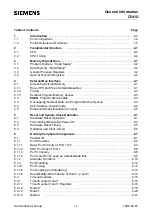
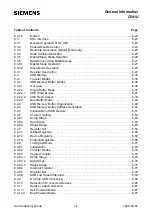
Page 2: ...s 1 2 1 2 1 2 1 4 1 5 1 6 to 1 9 1 5 3 1 3 5 3 7 3 8 6 1 6 34 6 53 6 56 6 58 6 61 6 75 6 78 7 2 7 7 7 11 7 12 10 3 10 4 to 10 5 Chapter 11 All chapters All chapters 1 2 1 2 1 2 1 4 1 5 1 5 to 1 8 1 5 3 1 3 5 3 7 3 8 6 1 6 34 6 53 6 56 6 58 6 61 6 75 6 88 7 2 7 7 7 12 7 13 10 3 10 3 to 10 4 All references to C540U is removed VCC is changed to VDD USB feature list Compliant to USB Specification Rev ...

Page 3: ...used in a life support device or system whose failure can reasonably be expected to cause the failure of that life support device or system or to affect its safety or effectiveness of that device or system 2 Life support devices or systems are intended a to be implanted in the human body or b to support and or maintain and sustain human life If they fail it is reasonable to assume that the health ...

Page 4: ...4 4 ALE Address Latch Enable 4 4 4 5 Enhanced Hooks Emulation Concept 4 5 5 Reset and System Clock Operation 5 1 5 1 Hardware Reset Operation 5 1 5 2 Fast Internal Reset after Power On 5 3 5 3 Hardware Reset Timing 5 5 5 4 Oscillator and Clock Circuit 5 6 6 On Chip Peripheral Components 6 1 6 1 Parallel I O 6 1 6 1 1 Port Structures 6 2 6 1 1 1 Basic Port Circuirty of Port 1 to 3 6 3 6 1 1 2 SSC P...

Page 5: ...Access 6 39 6 4 2 3 Dual Buffer Mode 6 42 6 4 3 USB Memory Buffer Organization 6 49 6 4 4 USB Memory Buffer Address Generation 6 50 6 4 5 Initialization of USB Module 6 51 6 4 6 Control Transfer 6 53 6 4 6 1 Setup Stage 6 53 6 4 6 2 Data Stage 6 53 6 4 6 3 Status Stage 6 53 6 4 7 Register Set 6 54 6 4 7 1 Global Registers 6 55 6 4 7 2 Device Registers 6 59 6 4 7 3 Endpoint Registers 6 66 6 4 8 Low...

Page 6: ...nd Watchdog Status Flag 8 4 8 2 Oscillator Watchdog Unit 8 5 8 2 1 Functionality of the Oscillator Watchdog Unit 8 6 8 2 2 Fast Internal Reset after Power On 8 7 9 Power Saving Modes 9 1 9 1 Idle Mode 9 3 9 1 1 Entering Idle Mode 9 4 9 1 2 Exit from Idle Mode 9 4 9 2 Power Down Mode 9 5 9 2 1 Entering Power Down Mode 9 6 9 2 2 Exit from Power Down Mode 9 7 9 2 2 1 Exit via Pin P3 2 INT0 9 8 9 2 2 ...

Page 7: ......

Page 8: ...mode The five endpoints can be easily controlled by the CPU via special function registers Due to the on chip USB transceiver circuits the C541U can be directly connected to the USB bus Figure 1 1 shows the different functional units of the C541U and figure 1 2 shows the simplified logic symbol of the C541U Figure 1 1 C541U Functional Units T0 T1 CPU Port 0 Port 1 Port 2 Port 3 I O I O OTP Prog Me...

Page 9: ...v1 0 Full speed or low speed operation Five endpoints one bidirectional control endpoint four versatile programmable endpoints Registers are located in special function register area On chip USB transceiver SSC synchronous serial interface SPI compatible Master and slave capable Programmable clock polarity clock edge to data phase relation LSB MSB first selectable 1 5 MBaud transfer rate at 12 MHz...

Page 10: ...r Group 1 3 1997 10 01 Introduction C541U Figure 1 2 Logic Symbol Port 0 8 bit Digital I O RESET EA ALE PSEN XTAL2 XTAL1 Port 1 6 bit Digital I O Port 2 8 bit Digital I O Port 3 8 bit Digital I O VSS VDD D D C541U ...

Page 11: ...12 13 14 15 16 17 5 4 3 2 1 44 43 42 41 40 39 38 37 36 35 34 33 32 31 30 29 18 19 20 21 22 23 24 25 26 27 P1 1 LED1 P1 0 LED0 D D ECAP V DDU P1 2 SCLK VDD VSS P3 0 LED2 P3 1 DADD P3 2 INT0 P3 3 INT1 P3 4 T0 P3 5 T1 P3 6 WR P3 7 RD XTAL2 XTAL1 V SS V DD P2 0 A8 P2 1 A9 P2 2 A10 P2 3 A11 P2 4 A12 RESET P0 3 AD3 P0 2 AD2 P0 1 AD1 P0 0 AD0 P0 4 AD4 P0 5 AD5 P0 6 AD6 P0 7 AD7 EA P1 4 STO PSEN P2 7 A15 ...

Page 12: ...g externally pulled low will source current I IL in the DC characteristics because of the internal pullup resistors Port 1 also contains two outputs with LED drive capability as well as the four pins of the SSC The pins with LED drive capability are able to sink current up to 10 mA The output latch corresponding to a secondary function must be programmed to a one 1 for that function to operate exc...

Page 13: ... of port 3 as follows P3 0 LED2 LED2 output P3 1 DADD Device attached input P3 2 INT0 External interrupt 0 input timer 0 gate control input P3 3 INT1 External interrupt 1 input timer 1 gate control input P3 4 T0 Timer 0 counter input P3 5 T1 Timer 1 counter input P3 6 WR WR control output latches the data byte from port 0 into the external data memory P3 7 RD RD control output enables the external...

Page 14: ... fetch operations It is activated every three oscillator periods except during external data memory accesses The signal remains high during internal program execution ALE 33 O The Address Latch enable output is used for latching the address into external memory during normal operation It is activated every three oscillator periods except during an external data memory access EA 35 I External Acces...

Page 15: ...value of the capacitor is 6 nF VDDU 1 Supply voltage for the on chip USB transceiver circuitry VDD 8 23 Supply voltage for ports and internal logic circuitry during normal idle and power down mode VSS 9 22 Ground 0V during normal idle and power down mode I Input O Output Table 1 1 Pin Definitions and Functions cont d Symbol Pin Numbers I O Function P LCC 44 C541U 2 VSS C ...

Page 16: ...e a versatile USB module as well as some enhancements in the Fail Save Mechanism Unit Figure 2 1 shows a block diagram of the C541U Figure 2 1 Block Diagram of the C541U Port 0 8 bit digit I O Port 2 8 bit digit I O Port 3 8 bit digit I O Port 0 Port 1 Port 2 Port 3 OSC Timing CPU Timer 0 Interrupt Unit XTAL2 XTAL1 RESET ALE PSEN EA Port 1 6 bit digit I O 256 x 8 RAM Timer Progr Watchdog Emulation...

Page 17: ...tion of data transfers and control the ALU processing The arithmetic section of the processor performs extensive data manipulation and is comprised of the arithmetic logic unit ALU an A register B register and PSW register The ALU accepts 8 bit data words from one or two sources and generates an 8 bit result under the control of the instruction decoder The ALU performs the arithmetic operations ad...

Page 18: ...set This causes the stack to begin a location 08H above register bank zero The SP can be read or written under software control Bit Function CY Carry Flag Used by arithmetic instruction AC Auxiliary Carry Flag Used by instructions which execute BCD operations F0 General Purpose Flag RS1 RS0 Register Bank select control bits These bits are used to select one of the four register banks OV Overflow F...

Page 19: ...nd phases Since these internal clock signals are not user accessible the XTAL2 oscillator signals and the ALE address latch enable signal are shown for external reference ALE is normally activated twice during each machine cycle once during S1P2 and S2P1 and again during S4P2 and S5P1 Executing of a one cycle instruction begins at S1P2 when the op code is latched into the instruction register If i...

Page 20: ...Cycle Instruction e g INC A Opcode Again Read Next b 2 Byte 1 Cycle Instruction e g ADD A DATA Read Opcode S1 S2 Byte Read 2nd S4 S3 S5 S6 Opcode Read Next S6 S5 S3 S4 S2 S1 Opcode Read Read Next Opcode Discard S1 S2 S4 S3 S5 S6 Read Next Opcode Again c 1 Byte 2 Cycle Instruction e g INC DPTR d MOVX 1 Byte 2 Cycle S4 S1 S2 S3 S5 S6 S1 S3 S2 S4 S5 S6 Read Opcode MOVX Discard Opcode Read Next No Fet...

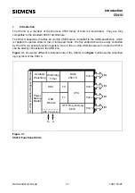
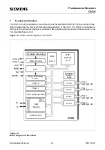
Page 21: ...Semiconductor Group 2 6 1997 10 01 Fundamental Structure C541U ...

Page 22: ...emory up to 64 Kbyte of external data memory 256 bytes of internal data memory a 128 byte special function register area Figure 3 1 illustrates the memory address spaces of the C541U Figure 3 1 C541U Memory Map FFFFH 2000H 1FFFH 0000H Code Space Internal EA 1 External EA 0 External Data Space Internal Data Space Indirect Direct External 0000H addr 7FH 00H Internal RAM Special Function Regs 80H FFH...

Page 23: ...The stack can be located anywhere in the internal data memory address space and the stack depth can be expanded up to 256 bytes The external data memory can be expanded up to 64 Kbyte and can be accessed by MOVX instructions that use a 16 bit or an 8 bit address Note The registers of the USB module are accessed through special function registers in the SFR area 3 3 General Purpose Registers The lo...

Page 24: ...The registers except the program counter and the four general purpose register banks reside in the special function register area All SFRs with addresses where address bits 0 2 are 0 e g 80H 88H 90H 98H F8H FFH are bitaddressable The 75 special function registers SFRs in the SFR area include pointers and registers that provide an interface between the CPU and the other on chip peripherals The SFRs...

Page 25: ...XX1010B 2 Ports P0 P1 P2 P3 Port 0 Port 1 Port 2 Port 3 80H 1 90H 1 A0H 1 B0H 1 FFH FFH FFH FFH Timer 0 Timer 1 TCON TH0 TH1 TL0 TL1 TMOD Timer 0 1 Control Register Timer 0 High Byte Timer 1 High Byte Timer 0 Low Byte Timer 1 Low Byte Timer Mode Register 88H 1 8CH 8DH 8AH 8BH 89H 00H 00H 00H 00H 00H 00H SSC Interface SSCCON STB SRB SCF SCIEN SSCMOD SSC Control Register SSC Transmit Buffer SSC Rece...

Page 26: ... Enable Register USB Endpoint n Interrupt Request Register USB Endpoint n Base Address Register USB Endpoint n Buffer Length Register USB Power Down Register USB Control Register USB Data Register 0 USB Data Register 1 USB Data Register 2 USB Data Register 3 USB Data Register 4 USB Data Register 5 USB Data Register 6 USB Data Register 7 D2H D3H D4H D6H C1H C2H C3H C4H C6H C7H C1H C2H C3H C4H C5H C...

Page 27: ...0 GATE C T M1 M0 8AH TL0 00H 7 6 5 4 3 2 1 0 8BH TL1 00H 7 6 5 4 3 2 1 0 8CH TH0 00H 7 6 5 4 3 2 1 0 8DH TH1 00H 7 6 5 4 3 2 1 0 90H 2 P1 FFH 7 6 SLS STO SRI SCLK LED1 LED0 93H SSCCON 07H SCEN TEN MSTR CPOL CPHA BRS2 BRS1 BRS0 94H STB XXH 7 6 5 4 3 2 1 0 95H SRB XXH 7 6 5 4 3 2 1 0 96H SSCMOD 00H LOOPB TRIO 0 0 0 0 0 LSBSM 9AH ITCON XXXX 1010B I1ETF I1ETR I0ETF I0ETR A0H 2 P2 FFH 7 6 5 4 3 2 1 0 A...

Page 28: ...1 LEN0 E8H 7 USBDR0 00H 7 6 5 4 3 2 1 0 E9H 7 USBDR1 00H 7 6 5 4 3 2 1 0 EAH 7 USBDR2 00H 7 6 5 4 3 2 1 0 EBH 7 USBDR3 00H 7 6 5 4 3 2 1 0 ECH 7 USBDR4 00H 7 6 5 4 3 2 1 0 EDH 7 USBDR5 00H 7 6 5 4 3 2 1 0 EEH 7 USBDR6 00H 7 6 5 4 3 2 1 0 1 X means that the value is undefined and the location is reserved 2 Bit addressable special function registers 3 SFR is located in the mapped SFR area For access...

Page 29: ...located in the mapped SFR area For accessing this SFR bit RMAP in SFR SYSCON must be set 4 These are read only registers 5 The content of this SFR varies with the actual step of the C541U e g 01H for the first step 6 The reset value of ADROFF is valid only if USBVAL has not been read or written since the last hardware reset 7 These registers are only used in USB low speed operation Table 3 2 Conte...

Page 30: ...10 FNR9 FNR8 EPSEL 0XXX X000B Endpoint 0 Registers C1H EPBC0 00H STALL0 0 0 GEPIE0 SOFDE0 INCE0 0 DBM0 C2H EPBS0 20H UBF0 CBF0 DIR0 ESP0 SETRD0 SETWR0 CLREP0 DONE0 C3H EPIE0 00H AIE0 NAIE0 RLEIE0 DNRIE0 NODIE0 EODIE0 SODIE0 C4H EPIR0 11H ACK0 NACK0 RLE0 DNR0 NOD0 EOD0 SOD0 C5H EPBA0 00H PAGE0 0 0 0 A06 A05 A04 A03 C6H EPLEN0 0XXX XXXXB 0 L06 L05 L04 L03 L02 L01 L00 C7H reserved EPSEL 0XXX X001B En...

Page 31: ... SETWR3 CLREP3 DONE3 C3H EPIE3 00H AIE3 NAIE3 RLEIE3 DNRIE3 NODIE3 EODIE3 SODIE3 C4H EPIR3 10H ACK3 NACK3 RLE3 DNR3 NOD3 EOD3 SOD3 C5H EPBA3 00H PAGE3 0 0 0 A63 A52 A43 A33 C6H EPLEN3 0XXX XXXXB 0 L63 L53 L43 L33 L23 L13 L03 C7H reserved EPSEL 0XXX X100B Endpoint 4 Registers C1H EPBC4 00H STALL4 0 0 GEPIE4 SOFDE4 INCE4 0 DBM4 C2H EPBS4 20H UBF4 CBF4 DIR4 ESP4 SETRD4 SETWR4 CLREP4 DONE4 C3H EPIE4 0...

Page 32: ...as Data Address Bus When used for accessing external memory port 0 provides the data byte time multiplexed with the low byte of the address In this state port 0 is disconnected from its own port latch and the address data signal drives both FETs in the port 0 output buffers Thus in this application the port 0 pins are not open drain outputs and do not require external pullup resistors During any a...

Page 33: ... without MOVX PCL OUT valid PCL OUT valid PCL OUT valid PCL OUT valid ALE PSEN RD P2 a b P2 RD PSEN ALE valid PCL OUT valid DPL or Ri valid PCL OUT MOVX with B IN PCL OUT IN DATA IN IN DPH OUT OR P2 OUT One Machine Cycle One Machine Cycle OUT PCL S6 S5 S4 S3 S2 S1 S6 S5 S4 S3 S2 S1 MCT03220 S1 S2 S3 S4 S5 S6 S1 S2 S3 S4 S5 S6 OUT PCH PCH OUT OUT PCH PCH OUT OUT PCH INST INST INST INST P0 P0 INST I...

Page 34: ...rt 2 SFR depending on whether the external data memory access is a MOVX DPTR or a MOVX Ri 4 2 PSEN Program Store Enable The read strobe for external program memory fetches is PSEN It is not activated for internal program memory fetches When the CPU is accessing external program memory PSEN is activated twice every instruction cycle except during a MOVX instruction no matter whether or not the byte...

Page 35: ...ows to switch off the ALE output signal If the internal OTP program memory is used EA 1 and ALE is switched off by EALE 0 ALE will only go active during external data memory accesses MOVX instructions and code memory accesses with an address greater than 1FFFH for the C541U external code memory fetches If EA 0 the ALE generation is always enabled and the bit EALE has no effect After a hardware res...

Page 36: ...an EH IC and a compatible C500 are able to emulate all operating modes of the different versions of the C500 microcontrollers This includes emulation of ROM OTP memory ROM OTP memory with code rollover and ROMless modes of operation It is also able to operate in single step mode and to read the SFRs after a break Figure 4 2 Basic C500 MCU Enhanced Hooks Concept Configuration Port 0 port 2 and some...

Page 37: ...Semiconductor Group 4 6 1997 10 01 External Bus Interface C541U ...

Page 38: ...nd machine cycle and is repeated every cycle until RESET goes low again During reset pins ALE and PSEN are configured as inputs and should not be stimulated or driven externally An external stimulation at these lines during reset activates several test modes which are reserved for test purposes This in turn may cause unpredictable output operations at several port pins At the RESET pin a pulldown ...

Page 39: ...by a reset After power up the content is undefined while it remains unchanged during a reset if the power supply is not turned off A reset operation of the USB module in the C541U can only be achieved under software control A hardware reset operation puts only the internal CPU interface of the USB module and its MMU into a well defined reset state The software reset which must be executed after a ...

Page 40: ... g 1 µs measured from VDD 4 25 V up to stable port condition the delay between power on and the correct port reset state is Typ 18 µs Max 34 µs The RC oscillator will already run at a VDD below 4 0V lower specification limit Therefore at slower VDD rise times the delay time will be less than the two values given above After the on chip oscillator has finally started the oscillator watchdog detects...

Page 41: ...627 I II III IV V Power On undef Ports typ 18 max 34 µ s µ s Clock from RC Oscillator RESET at Ports On Chip Osc starts Sequence Final RESET by Osc WD max 768 RC in RESET Port remains because of active ext Execution Start of Program RESET Undef Ports On Chip Osc RC Osc V RESET CC RESET Signal Clock Cycles ...

Page 42: ...for performing a perfect reset without clock at the XTAL1 and XTAL2 pins The RESET signal must be active for at least two machine cycles after this time the C541U remains in its reset state as long as the signal is active When the signal goes inactive this transition is recognized in the following state 5 phase 2 of the machine cycle Then the processor starts its address output when configured for...

Page 43: ...ed by bit PCLK of SFR DCR Depending on full or low speed operation of the USB bit SPEED of SFR has to be set or cleared for the selection of the USB clock Bit UCLK is a general enable bit for the USB clock Figure 5 4 Block Diagram of the Clock Generation Circuitry In low speed mode the PLL is not required Therefore the PLL should be always disabled in low speed mode This also reduces the power con...

Page 44: ... and output of a single stage on chip inverter which can be configured with off chip components as a Pierce oscillator The oscillator in any case drives the internal clock generator The clock generator provides the internal clock signals to the chip These signals define the internal phases states and machine cycles Figure 5 5 shows the recommended oscillator circuit Figure 5 5 Recommended Crystal ...

Page 45: ...be applied to XTAL1 as shown in figure 5 7 XTAL2 has to be left unconnected A pullup resistor is suggested to increase the noise margin but is optional if VOH of the driving gate corresponds to the VIH2 specification of XTAL1 Figure 5 7 External Clock Source XTAL2 XTAL1 To Internal Timing Circuitry C541U C 2 C 1 MCD03395 C540U 12 MHz External Clock Signal VDD N C XTAL2 XTAL1 C541U ...

Page 46: ...pulled high and will source current when externally pulled low Port 0 will float when configured as input The output drivers of port 0 and 2 and the input buffers of port 0 are also used for accessing external memory In this application port 0 outputs the low byte of the external memory address time multiplexed with the byte being written or read Port 2 outputs the high byte of the external memory...

Page 47: ... The bit latch one bit in the port s SFR is represented as a type D flip flop which will clock in a value from the internal bus in response to a write to latch signal from the CPU The Q output of the flip flop is placed on the internal bus in response to a read latch signal from the CPU The level of the port pin itself is placed on the internal bus in response to a read pin signal from the CPU Som...

Page 48: ...ust contain a one 1 that means for figure 6 2 Q 0 which turns off the output driver FET n1 Then for ports 1 2 and 3 the pin is pulled high by the internal pullups but can be pulled low by an external source When externally pulled low the port pins source current IIL or ITL For this reason these ports are sometimes called quasi bidirectional Figure 6 2 Basic Output Driver Circuit of Ports 1 2 and 3...

Page 49: ...ansition of the logic levels at the pin The pullup FET p2 is of p channel type It is always activated when a 1 is in the port latch thus providing the logic high output level This pullup FET sources a much lower current than p1 therefore the pin may also be tied to ground e g when used as input with logic low input level The pullup FET p3 is of p channel type It is only activated if the voltage at...

Page 50: ...f power on reset the pins will be in IL state latch is set to 1 voltage level on pin is below of the trip point of p3 Depending on the voltage level and load applied to the pin it will remain in this state or will switch to IH SOH state If it is is used as output the weak pull up p2 will pull the voltage level at the pin above p3 s trip point after some time and p3 will turn on and provide a stron...

Page 51: ...r SLCK and STO Pin Control for P1 2 SCLK When the SSC is disabled both Enable Push pull and Tristate will be inactive the pin behaves like a standard I O pin In master mode and with SSC enabled Enable Push pull will be active and Tristate will be inactive In slave mode and with SSC enabled Enable Push pull will be inactive and Tristate will be active Pin Control for P1 4 STO When the SSC is disabl...

Page 52: ...nputs used for the SSC will be switched into a high impedance mode For P1 3 SRI Tristate will be enabled when the SSC is enabled For P1 5 SLS Tristate will be enabled when the SSC is enabled and is switched to slave mode In master mode this pin will remain a regular I O pin MCS02433 1 1 1 VCC Port Pin SS V Q Tristate Input Data Read Pin Delay 1 State p1 p2 p3 n1 1 _ 1 _ 1 _ ...

Page 53: ...the port is emitting 1 s during the external memory accesses Otherwise the pullup is always off Consequently P0 lines that are used as output port lines are open drain lines Writing a 1 to the port latch leaves both output FETs off and the pin floats In that condition it can be used as high impedance input If port 0 is configured as general I O port and has to emit logic high level 1 external pull...

Page 54: ...ut level at the EA pin and or the contents of the program counter If the ports are configured as an address data bus the port latches are disconnected from the driver circuit During this time the P2 SFR remains unchanged while the P0 SFR has 1 s written to it Being an address data bus port 0 uses a pullup FET as shown in figure 6 6 When a 16 bit address is used port 2 uses the additional strong pu...

Page 55: ...function to the output pin and vice versa however the gate between the latch and driver circuit must be open Thus to use the alternate input or output functions the corresponding bit latch in the port SFR has to contain a one 1 otherwise the pulldown FET is on and the port pin is stuck at 0 After reset all port latches contain ones 1 Figure 6 8 Circuitry of Ports 1 and 3 MCS01827 D CLK Bit Latch Q...

Page 56: ... T2 T2EX SCLK SRI STO SLS DADD INT0 INT1 T0 T1 WR RD Input to counter 2 Capture reload trigger of timer 2 up down count SSC master clock output slave clock input SSC serial data input SSC serial data output SSC slave select input Device attached input of the USB module External interrupt 0 input timer 0 gate control External interrupt 1 input timer 1 gate control Timer 0 external counter input Tim...

Page 57: ... A P1 the port pin is actually sampled in state 5 phase 1 or phase 2 depending on port and alternate functions Figure 6 9 illustrates this port timing lt must be noted that this mechanism of sampling once per machine cycle is also used if a port pin is to detect an edge e g when used as counter input In this case an edge is detected when the sampled value differs from the value that was sampled th...

Page 58: ...re VOL and VOH The same applies to port 0 output buffers They do however require external pullups to drive floating inputs except when being used as the address data bus When used as inputs it must be noted that the ports 1 2 and 3 are not floating but have internal pullup transistors The driving devices must be capable of sinking a sufficient current if a logic low level shall be applied to the p...

Page 59: ... byte back to the latch The reason why read modify write instructions are directed to the latch rather than the pin is to avoid a possible misinterpretation of the voltage level at the pin For example a port bit might be used to drive the base of a transistor When a 1 is written to the bit the transistor is turned on If the CPU then reads the same port bit at the pin rather than the latch it will ...

Page 60: ...e of the external input signal but to ensure that a given level is sampled at least once before it changes it must be held for at least one full machine cycle 6 2 1 Timer Counter 0 and 1 Timer counter 0 and 1 of the C541U are fully compatible with timer counter 0 and 1 of the 80C51 C501 and can be used in the same four operating modes Mode 0 8 bit timer counter with a divide by 32 prescaler Mode 1...

Page 61: ...ddress 8DH Reset Value 00H Bit Function TLx 7 0 x 0 1 Timer counter 0 1 low value THx 7 0 x 0 1 Timer counter 0 1 high value 7 6 5 4 8AH TL0 Bit No 7 6 5 4 3 2 1 0 MSB LSB 3 2 1 0 7 6 5 4 8CH TH0 3 2 1 0 7 6 5 4 8BH TL1 3 2 1 0 7 6 5 4 8DH TH1 3 2 1 0 Operating Mode Description 0 TLx holds the 5 bit prescaler value 1 TLx holds the lower 8 bit part of the 16 bit timer counter value 2 TLx holds the ...

Page 62: ... timer counter overflow Cleared by hardware when processor vectors to interrupt routine TR1 Timer 1 run control bit Set cleared by software to turn timer counter 1 ON OFF TF1 Timer 1 overflow flag Set by hardware on timer counter overflow Cleared by hardware when processor vectors to interrupt routine 8FH 8EH 8DH 8CH 8BH 8AH 89H 88H TF1 TR1 TF0 TR0 88H TCON Bit No 7 6 5 4 3 2 1 0 MSB LSB IE1 IT1 I...

Page 63: ...eration input from internal system clock M1 M0 Timer 1 0 mode select bits Gate C T M1 M0 89H TMOD Bit No 7 6 5 4 3 2 1 0 MSB LSB Gate C T M1 M0 Timer 1 Control Timer 0 Control M1 M0 Function 0 0 8 bit timer counter THx operates as 8 bit timer counter TLx serves as 5 bit prescaler 0 1 16 bit timer counter THx and TLx are cascaded there is no prescaler 1 0 8 bit auto reload timer counter THx holds a...

Page 64: ...n TR0 1 and either Gate 0 or INT0 1 setting Gate 1 allows the timer to be controlled by external input INT0 to facilitate pulse width measurements TR0 is a control bit in the special function register TCON Gate is in TMOD The 13 bit register consists of all 8 bits of TH0 and the lower 5 bits of TL0 The upper 3 bits of TL0 are indeterminate and should be ignored Setting the run flag TR0 does not cl...

Page 65: ...04 01 On Chip Peripheral Components C541U 6 2 1 3 Mode 1 Mode 1 is the same as mode 0 except that the timer register is running with all 16 bits Mode 1 is shown in figure 6 11 Figure 6 11 Timer Counter 0 Mode 1 16 Bit Timer Counter ...

Page 66: ... the timer register as an 8 bit counter TL0 with automatic reload as shown in figure 6 12 Overflow from TL0 not only sets TF0 but also reloads TL0 with the contents of TH0 which is preset by software The reload leaves TH0 unchanged Figure 6 12 Timer Counter 0 1 Mode 2 8 Bit Timer Counter with Auto Reload ...

Page 67: ...s C T Gate TR0 INT0 and TF0 TH0 is locked into a timer function counting machine cycles and takes over the use of TR1 and TF1 from timer 1 Thus TH0 now controls the timer 1 interrupt Mode 3 is provided for applications requiring an extra 8 bit timer or counter When timer 0 is in mode 3 timer 1 can be turned on and off by switching it out of and into its own mode 3 or can still be used by the seria...

Page 68: ...lex operation and can run in a master or a slave mode Figure 6 14 shows the block diagram of the SSC The central element of the SSC is an 8 bit shift register The input and the output of this shift register are each connected via a control logic to the pin P1 3 SRI SSC Receiver In and P1 4 STO SSC Transmitter Out This shift register can be written to SFR STB and can be read through the Receive Buf...

Page 69: ... with the clock signal at pin SCLK When the eight bits are shifted out and the same number is of course shifted in the contents of the shift register is transferred to the receive buffer register SRB and the transmission complete flag TC is set If enabled an interrupt request will be generated After the last bit has been shifted out and was stable for one bit time the STO output will be switched t...

Page 70: ...ock transisition will not occur before one half transmit clock cycle time after the register load This ensures that there is sufficient setup time between MSB or LSB valid on the data output and the first sample clock edge and that the MSB or LSB has the same length than the other bits No special care is necessary in case of CPHA 1 because here the first clock edge will be used for shifting 6 3 4 ...

Page 71: ...ster or as slave unit The SSC has no on chip support for multimaster configurations switching between master and slave mode operation Operating the SSC as a master in a multimaster environment requires external circuitry for swapping transmit and receive lines Figure 6 15 Typical SSC System Configuration Master SSC SCLK STO SRI Px x Px y Px z SCLK SRI STO SLS Slave SSC Dedicated Slave Select Lines...

Page 72: ...h the next clock edge The direction rising or falling of the respective clock edge is depending on the clock polarity selected After the last bit has been shifted out the data output STO will go to the high output level logic 1 and remain there until the next transmission is started However when enabling the SSC after reset the logic level of STO will be undefined until the first transmission star...

Page 73: ...the input with the first clock edge and the transmitter will shift out the next bit with the following clock edge If the transmitter is disabled the output will remain in the high impedance state In this case CPHA 0 correct operation requires that the SLS input to go inactive between consecutive bytes When SLS is inactive the internal shift clock is disabled and the content of the shift register w...

Page 74: ... 95H 96H Bit Function SCEN SSC system enable SCEN 0 SSC subsystem is disabled related pins are available as general I O SCEN 1 SSC subsystem is enabled TEN Slave mode transmitter enable TEN 0 Transmitter output STO will remain in tristate state regardless of the state of SLS TEN 1 and SLS 0 Transmitter will drive the STO output In master mode the transmitter will be enabled all the time regardless...

Page 75: ...le the data the second to shift the next bit out at STO In master mode the transmitter will provide the first data bit on STO immediately after the data was written into the STB register In slave mode the transmitter if enabled via TEN will shift out the first data bit with the falling edge of SLS CPHA 1 The first data bit is shifted out with the first clock edge of SCLK and sampled with the secon...

Page 76: ...ted by bit ESSC in the interrupt enable register IEN2 and by bit 2 in the interrupt priority registers IP0 and IP1 Bit Function Reserved for future use WCEN SSC write collision interrupt enable WCEN 0 No interrupt request will be generated if the WCOL bit in the status register SCF is set WCEN 1 An interrupt is generated if the WCOL bit in the status register SCF is set TCEN SSC transfer completed...

Page 77: ...If WCOL is set it indicates that an attempt was made to write to the shift register STB while a data transfer was in progress and not fully completed This bit will be set at the trailing edge of the write signal during the erronous write attempt This bit can be reset in two different ways 1 writing a 0 to the bit bit access byte access or read modify write access 2 by reading the bit or the status...

Page 78: ...a an inverter to the SRI input allowing to check the transfer locally without a second SSC device TRIO SSC disable tristate mode of SSC inputs This bit should be used for test purposes only TRIO 0 The SSC operates as specified TRIO 1 The SSC inputs will be connected to the output latch of the corresponding port pin This allows a test of the SSC in slave mode by simulating a transfer via a program ...

Page 79: ...B specific special function registers and the interrupt control logic A clock generation unit provides the clock signal for the USB module for full speed and low speed USB operation The following sections describe the full speed operation while the low speed operation is described specifically in section 6 4 8 Figure 6 18 shows the block diagram of the functional units of the USB module with their...

Page 80: ...onfigured as control endpoint with a maximum buffer length of 8 bytes The control endpoint can be configured to handle data packets of 64 bytes maximum length Isochronous full speed mode only Isochronous data are continuous and real time in creation and consumption such as voice data In this case real time is defined from frame to frame Isochronous data transfer has the highest priority but is not...

Page 81: ...fer mode Random access allows to change only a few bytes in a data block of the USB memory buffer When the CPU has modified the bytes in the data block setting of bit DONE by software marks the buffer ready for transmission or reception of data over the USB pipe For modification of a specific byte in the buffer the CPU must write the address to SFR ADROFF and read write the data byte from to regis...

Page 82: ...ndpoint can be stored permanently in USB memory As a result an additional memory space for data storage is no longer needed 6 4 2 2 1 USB Write Access Figure 6 20 shows the basic flowchart of a USB write access to one USB memory buffer in single buffer mode Figure 6 20 USB Write Access in Single Buffer Mode Buffer Handling Buffer is empty USB write access enabled CPU read access disabled No CPU re...

Page 83: ...PU can read data bytes from USB memory generating an EOD end of data at after the last byte has been read Bit EOD set indicates an empty USB buffer which now can be written again by the USB Figure 6 21 also shows a second USB write access operation with a different number of bytes Len n 1 where the CPU read operation from the USB memory is interrupted twice Figure 6 21 Single Buffer Mode Standard ...

Page 84: ...B memory buffer in single buffer mode Figure 6 22 USB Read Access in Single Buffer Mode Buffer Handling Buffer is empty USB read access disabled CPU write access enabled Buffer can be written by CPU Buffer full No CPU write access disabled USB read access enabled Buffer is full EOD 1 USB read request No Buffer empty Buffer is read by USB No SOD 1 MCD03402 Yes Yes Yes ...

Page 85: ...set by software The MaxLen value must be previously set by software When the actual USB memory buffer address offset is equal to MaxLen bit EOD is set at to indicate a full buffer The USB memory buffer address offset is automatically incremented with every CPU write access to USB memory buffer if bit INCE is set During the next frame after SOF n 1 is set at the USB memory buffer can be read by the...

Page 86: ...tomatic setting of bit SOF causes bit EOD to be set at This indicates the CPU that no CPU action on this buffer is required until a USB read operation has been finished bit SOD set at Setting of SOD indicates an empty USB memory to the CPU which can start again writing data into USB memory Figure 6 24 Single Buffer Mode USB Read Access with Start of Frame Done Enabled 1 2 1 SOD set 2 Frame n Frame...

Page 87: ...uffer mode for the USB read access and USB write access Figure 6 25 USB Read Access in Dual Buffer Mode Buffer Handling CPU Buffer Handling CPU page is empty CBF 0 CPU write access enabled CPU writes 1 Byte CPU buffer full CPU buffer is full CBF 1 CPU write access disabled Pages are CBF 1 and UBF 0 EOD 1 USB page empty SOD 1 Yes Yes No No No Yes Yes full CPU page USB read access disabled USB buffe...

Page 88: ... 1 CPU read access enabled CPU reads 1 Byte CPU buffer empty CPU buffer is empty CBF 0 CPU read access disabled Pages are CBF 0 and UBF 1 EOD 1 USB page full SOD 1 Yes Yes No No No Yes Yes empty CPU page USB write access disabled USB buffer is full UBF 1 request USB write USB writes buffer USB write access enabled USB page is empty UBF 0 USB Buffer Handling No MCB03406 swapped ...

Page 89: ...e USB is empty again with UBF 0 During the USB read access the CPU is still allowed to write into its assigned buffer When reaching MaxLen at the CPU buffer is full and both buffers are again logically swapped The USB further execute its read access Figure 6 27 Dual Buffer Mode USB Read Access Buffer Switching when MaxLen is reached In dual buffer mode the physical assignment of the USB memory pag...

Page 90: ... is not changed when bit DONE is set The actual packet length Len1 or Len2 is the number of bytes which have been written to the buffer before bit DONE is set Figure 6 28 Dual Buffer Mode USB Read Access Buffer Switching by Setting Bit DONE Frame n Frame n 1 Time SOF n set Number of Data Bytes MaxLen USB read accesses CPU write accesses MCT03408 DONE 1 Len1 SOF n 2 set Time SOF n 1 set 1 3 Page 0 ...

Page 91: ...ed to USB is empty again UBF 0 and can be swapped again as soon as the CPU has filled its buffer at The number of bytes in the buffer is less or equal MaxLen The MaxLen threshold is always active but an occurrence of SOF if SOFDE 1 or setting bit DONE by software are used to tag the CPU buffer full before reaching MaxLen Figure 6 29 Dual Buffer Mode USB Read Access Buffer Switching on SOF with SOF...

Page 92: ...the complete data packet has been written to the buffer by the CPU bit DONE is set by software to indicate the end of the data packet CBF 1 In the example the USB buffer has not been read out It is still full for the USB and can not be swapped CBF UBF 1 When the USB read access has occured CBF 0 the buffers are automatically swapped and bit SOD is set Figure 6 30 Double Buffer Mode USB Read Access...

Page 93: ...ing is initiated This action is independent from the number of bytes which have been handled by the CPU possible in sequential access mode INCE 1 and random access mode INCE 0 On CPU read accesses the buffer is declared empty and bit CBF is cleared If the buffer assigned to the USB is full UBF 1 the buffers are immediately swapped In this case register EPLENn contains the number of received bytes ...

Page 94: ...packet is always located at address 00H This leads to a typical USB buffer structure as shown in figure 6 31 with a buffer length of 64 bytes for endpoint 2 16 bytes for endpoints 1 and 3 8 bytes for endpoint 0 and a predefined length of 8 bytes for endpoint 0 and the setup token Figure 6 31 Endpoint Buffer Allocation Example 4 Endpoints Table 6 5 USB Buffer Length and Base Addresses Values Buffer...

Page 95: ...ently accessed byte in the USB memory area of the selected endpoint is defined by an address offset which must be added to the endpoint base address in order to get the correct address for the USB memory buffer The structure is shown in figure 6 32 Figure 6 32 USB Memory Address Generation With the software initialization of the USB module as described in section 6 4 5 each endpoint is initialized...

Page 96: ...nce The USB module must be functionally initialized from the CPU by writing five configuration bytes for each endpoint to the USBVAL register Thereafter bit DONE0 in register EPBS0 must be set by software Figure 6 33 shows the 5 byte configuration block which must be transmitted by the CPU to the USB module via the USBVAL register for each endpoint The gray shaded fields have a fixed 0 or 1 value ...

Page 97: ...k EPType This 2 bit field defines the type of the endpoint 00 Control endpoint 01 Isochronous endpoint 10 Bulk endpoint 11 Interrupt endpoint Endpoint 0 must be setup for control endpoint EPDir This bit defines the direction of the endpoint 0 Out packets to be transferred from Host to CPU 1 In packets to be transferred from CPU to Host EPPackSize This 10 bit field defines the maximum packet size t...

Page 98: ...his data stage is always predicted to be from Host to Device bit DIR is automatically cleared after the setup stage occured The first data packet may immediately be send from the Host to the control endpoint according to this configuration of bit DIR while NACK will be automatically returned from the Device to the Host in case of USB read access The configuration of bit DIR 0 predicts an USB write...

Page 99: ... 6 34 Register Structure of the USB Module Note In the description of the USB module registers bits are marked as rw r or w Bits marked as rw can be read and written Bits marked as r can be read only Writing any value to r bits has no effect Bits marked as w are used to execute internal commands which are triggered by writing a 1 Writing a 0 to w bits has no effect Reading w bits returns a 0 D Glo...

Page 100: ...t Select Register EPSEL Address D2H Reset Value 80H Bit Function EPS7 EPS2 EPS1 EPS0 Endpoint device register block select bits These four bits select the active register block of endpoint or device registers Table 6 7 shows the register definitions of each endpoint or device register block in detail MSB LSB EPSEL EPS7 0 0 0 0 EPS2 EPS1 EPS0 7 6 5 4 3 2 1 0 Bit No rw r r r r rw rw rw D2H EPS7 EPS2...

Page 101: ...gister Set Address Assignment EPSEL SFR Addr Selected Register 1XXXXXXXB Device register block selected C1H C2H C3H C4H C5H C6H C7H DCR Device Control Register DPWDR Device Power Down Register DIER Device Interrupt Enable Register DIRR Device Interrupt Request Register reserved address FNRL Frame Number Register low byte FNRH Frame Number Register high byte 0XXXXnnnB nnn 000B to 100B Endpoint nnnB...

Page 102: ...rite operation or DIR 1 and CBF 0 read operation USB Address Offset Register ADROFF Address D4H Reset Value 00H After each modification automatical or by write action of the address offset register ADROFF the value pointed to is automatically read out of USB memory and transferred to register USBVAL Bit Function AO5 0 USB address offset register AO5 0 stores the 6 bit offset address for USB memory...

Page 103: ... Device request value interrupt Bit DRVI is set each time the host sends device request that contains one or more of the following Configuration Value through SET_CONFIGURATION device request Alternate Setting through SET_INTERFACE device request Interface through SET_INTERFACE device request This flag can only be cleared by writing 0 to the bit Writing 1 to the bit will be ignored The device inte...

Page 104: ... 12 MBaud or low speed 1 5 MBaud mode This bit can only be written with bit SWR 1 software reset After hardware reset the USB module runs in low speed mode and the PLLx4 is automatically disabled If SPEED 0 low speed mode selected default after reset If SPEED 1 full speed mode selected DA Device attached Bit DA reflects the state of pin DADD which can be used to indicate whether the device is atta...

Page 105: ... setting bit RSM resumes bus activity of the device In response to this action the USB will disassert the suspend bit and will perform the remote wake up operation Writing 0 to RSM has no effect the bit is reset if bit SUSP is 0 UCLK UDC clock selection Bit UCLK controls the functionality of the USB core clock in full speed mode SPEED 1 as well as in low speed mode SPEED 0 If UCLK 0 the USB core c...

Page 106: ...VREG disables the default on chip voltage regulator This is recommended if using an external USB voltage regulator is intended If XVREG 0 the on chip regulator is enabled If XVREG 1 the on chip regulator is disabled 0 Reserved for future use For compatiblity these bits have to be ignored in all read accesses and written with zero in all write accesses TPWD USB Transmitter Power Down Setting bit TP...

Page 107: ... device attached interrupt is disabled If DAIE 1 the device attached interrupt is enabled DDIE Device detached interrupt enable Setting bit DDIE enables the generation of a device interrupt when it is detached from the USB bus If DDIE 0 the device detached interrupt is disabled If DDIE 1 the device detached interrupt is enabled SBIE Suspend begin interrupt enable Setting bit SBIE enables the gener...

Page 108: ...p packet which must be processed by the CPU If SUIE 0 the setup interrupt is disabled If SUIE 1 the setup interrupt is enabled SOFIE Start of frame interrupt enable bit SOFIE enables the generation of a device interrupt on the detection of a start of frame packet on the USB If SOFIE 0 the start of frame interrupt is disabled If SOFIE 1 the start of frame interrupt is enabled Bit Function ...

Page 109: ...errupt Bit SEI is automatically set when the suspend mode is left STI Status interrupt Bit STI is set if the host requests a status transfer and the device answers with NACK if bit ESP is set the device answers with ACK and STI is not set SUI Setup interrupt Bit SUI is automatically set after a successful reception of a setup packet which is not handled by the USB module and must be forwarded to t...

Page 110: ... a hardware reset Frame Number Register High Byte FNRH Address C7H Reset Value 00000XXXB Frame Number Register Low Byte FNRL Address C6H Reset Value XXH Bit Function FNR10 0 Frame number value FNRH 2 0 and FNRL 7 0 hold the current 11 bit frame number of the latest SOF token FNRL holds the lowest 8 bits while FNRH holds the upper 3 bits of the frame number MSB LSB FNRH 0 0 0 0 0 FNR10 FNR9 FNR8 7 ...

Page 111: ...If the stall bit for endpoint 0 STALL0 is set the next incoming setup token will automatically clear it GEPIEn Global endpoint interrupt enable Bit GEPIEn enables or disables the generation of the global endpoint interrupt n based on the endpoint specific interrupt request bits in register EPIRn If GEPIE 0 the USB endpoint n interrupt is disabled If GEPIE 1 the USB endpoint n interrupt is enabled ...

Page 112: ...er This allows the user to handle the USB memory like a FIFO without modification of the address of the desired memory location by software After each modification of ADROFF the data value pointed to is automatically read out of USB memory and transferred to the USBVAL register If INCE 0 the auto increment function is disabled If INCE 1 the auto increment function is enabled DBMn Dual buffer mode ...

Page 113: ... the last data flow for endpoint n was from host to CPU If DIRn 1 the last data flow for endpoint n was from CPU to host ESPn Enable status phase If bit ESPn is set the next status phase of endpoint n will automatically be acknowledged by an ACK except the endpoint n is stalled If the status phase was successfully completed bit ESPn is automatically reset by hardware and no status interrupt reques...

Page 114: ... the direction of endpoint n This means bit DIRn is not changed Note When bits CLREPn and ESPn are set simultaneously with one instruction bit ESPn remains set and the next status phase is enabled If only CLREPn is set bit ESPn is reset and the status phase is disabled Setting bits CLREPn and SETRDn or SETWRn simultaneously with one instruction is not allowed This means that the information of SET...

Page 115: ...IRn is set If NAIEn 0 the USB not acknowledged interrupt is disabled If NAIEn 1 the USB not acknowledged interrupt is enabled RLEIEn Read length error interrupt enable Bit RLEIEn enables the generation of an endpoint specific read length error interrupt when bit RLEn in register EPIRn is set If RLEIEn 0 the read length error interrupt is disabled If RLEIEn 1 the read length error interrupt is enab...

Page 116: ...Dn in register EPIRn is set If EODIEn 0 the end of data interrupt is disabled If EODIEn 1 the end of data interrupt is enabled SODIEn Start of data interrupt enable Bit SODIEn enables the generation of an endpoint specific start of data interrupt when bit SODn in register EPIRn is set If SODIEn 0 the start of data interrupt is disabled If SODIEn 1 the start of data interrupt is enabled Bit Functio...

Page 117: ... This bit is set by hardware if the UDC requires an access to USB memory but no buffer is available USB Read action DNRn is set if UBF is not set USB Write action DNRn is set if UBF is set NODn No data This bit indicates an incorrect CPU read or write access to USB memory It is set if the CPU processes a read access to an empty USB buffer or a write access to a full buffer NODn is also set if the ...

Page 118: ...Dn Start of data USB Read action SODn is set if the USB has read a fixed number USBLen of bytes from the transmit buffer As a result the buffer is empty now and the CPU can process write actions again USB Write action SODn is set if the USB has written a fixed number USBLen of bytes to the receive buffer As a result the buffer is full and the CPU can start read actions Bit Function ...

Page 119: ...0 PAGEn 0 or on USB memory buffer page 1 PAGEn 1 by clearing or setting this bit In dual buffer mode this bit has no effect Note The SETUP token is always stored on USB memory buffer page 0 at address 00H to 07H An6 An3 Endpoint n buffer start address The bits 0 to 3 of EPBAn are the address bits A6 to A3 of the USB memory buffer start address for endpoint n A7 and A2 A0 of the resulting USB memor...

Page 120: ...8 bytes fully direct accesible data packet Two supported transfer modes control transfer through EP0 interrupt transfer interval from 10 ms to 255 ms The low speed operation require a different set of registers than the full speed operation These registers are described in section 6 4 8 5 6 4 8 1 Initialization After a successful hardware reset the device is by default in USB low speed mode The in...

Page 121: ... Empty to the TYPE bit field Since C541U only supports single device configuration and single interface setting multiple device configuration through set_configuration and setting alternate interface through set_interface to the device will be ignored 6 4 8 3 2 Data Stage This stage is optional and defined only for requests that require data transfer The direction of the transfer is either from th...

Page 122: ...ng with programmable rate from 10 ms to 255 ms A no acknowledge handshake NACK is automatically returned to the host if the device has currently no interrupt data to transfer Software is required to set up the data packet in the USBDRn registers to set the LEN bit field according to the data length and to set the TYPE bit field to either 0110B for EP1 interrupt endpoint or 0111B for EP2 interrupt ...

Page 123: ...t has been received and the setup data is stored in the USBDRn registers and SETUP interrupt request is also generated A read operation to register USBDCR resets the pending interrupt request while TYPE bit field maintains its current value 0010B 0011 OUT packet An OUT packet has been received by endpoint zero and is stored in the USBDRn registers and OUT interupt request is generated A read opera...

Page 124: ... pending The bus is in suspended mode and the suspend interrupt is pending Current reading of this register clears the interrupt request 1011 Reset interrupt pending The device has received a reset signal and the reset interrupt is pending Current reading of this register clears the interrupt request 1100 DADD falling A falling edge was detected on DADD pin and the DADD interrupt has been cleared ...

Page 125: ...R register MOV R2 12H Move immediate data to R2 MOV USBDCR R2 Move the content of R2 into USBDCR register LEN3 0 Length Information contains the number of bytes currently stored in the USB data registers LEN is set to 1111B when the hardware accesing the USBDRn registers Bitfield LEN is updated either by USB or by CPU CPU The number of bytes packet size has to be written to bitfield LEN at the end...

Page 126: ...nd mode This bit is set when the USB has been idle for more than 3 ms It will remain set until there is a non idle state on the USB cable DADD Device attached or detached Bit DADD monitors the state of the associated I O pin DADD see also TYPE bit field of USBDCR TPWD Transmitter Power Down 0 Transmitter is active 1 Transmitter is in power down state RPWD Receiver Power Down 0 Receiver is active 1...

Page 127: ...n i e data 0 data 1 data n 2 data n 1 then the data should be arranged in the following manner USBDR0 data 0 USBDR1 data n 1 USBDR2 data n 2 USBDRn 1 data 1 MSB LSB USBDR3 7 6 5 4 3 2 1 0 Bit No rw rw rw rw 2 1 0 USBDR0 USBDR1 USBDR2 E8H E9H EAH EBH 7 6 5 4 3 rw rw rw rw rw rw rw rw 2 1 0 7 6 5 4 3 rw rw rw rw rw rw rw rw 2 1 0 7 6 5 4 3 rw rw rw rw rw rw rw rw 2 1 0 7 6 5 4 3 rw rw rw rw rw rw rw...

Page 128: ...1 register has to be enabled before using these interrupts The interrupts are cleared by reading USBDCR register The following table lists the USB Low Speed specific interrupts Table USB Low Speed Interrupt Source and Vectors Interrupt Request Interrupt Enable Flags SETUP packet interrupt OUT packet interrupt USB Suspend interrupt USB Reset interrupt DADD interrupt always enabled always enabled SU...

Page 129: ...ve 2 8 V with a 15 kΩ load to VSS The driver outputs support tri state operation to achieve bi directional half duplex operation control bits RPWD and TPWD High impedance is also required to isolate the port from devices that are connected but powered down The driver tolerates a voltage on the signal pins of 0 5 V to 3 8 V with respect to local ground reference without damage This voltage is toler...

Page 130: ...smooth rise and fall times and minimal reflections and ringing when driving the USB cable see figure 6 37 This cable and driver are used only on network segments between low speed devices and the ports to which they are connected Figure 6 37 Low Speed USB Driver Signal Waveforms One Bit Time 12 MB s One Way Trip Cable Delay VSS Receiver Signal Pins Signal Pins Driver Signal Pins Pass Input Spec Le...

Page 131: ... than 2 5 µs 30 full speed data bit times When a device is detached from the USB the pull down resistors will cause both D and D lines to be pulled below the single ended low threshold of the host or hub port This creates a state called a single ended zero SE0 on the downstream port A disconnect condition is indicated if an SE0 persists on a downstream port for more than 2 5 µs 30 full speed data ...

Page 132: ...SFR DIRR and can generate a device interrupt too 6 4 11 2 Bus Powered Mode In bus powered mode the USB device is driven by the power supply from the USB bus The maximum power consumption is given by the USB specification In order to respect this specification the power consumption in suspend mode should not exceed 500 µA An explicit device attached detection in this mode is not necessary If the CP...

Page 133: ...Semiconductor Group 6 88 1999 04 01 On Chip Peripheral Components C541U ...

Page 134: ...ive a general overview of the interrupt sources and illustrate the request and control flags which are described in the next sections Figure 7 1 Interrupt Request Sources Part 1 EA ET0 TF0 IEN0 1 TCON 5 000BH IEN0 7 Low Priority MCT03684 Bit addressable Request flag is cleared by hardware IP0 1 PT0 High Priority TCON 7 TF1 ET1 IEN0 3 H 001B Timer 1 Timer 0 IEN0 0 TCON 1 IE0 0003 EX0 H Overflow Ove...

Page 135: ...ter has been read Endpoint 0 Interrupts 1 ACK0 NACK0 RLE0 DNR0 NOD0 EOD0 AIE0 EPIE0 7 NAIE0 EPIE0 6 RLEIE0 EPIE0 5 DNRIE0 EPIE0 3 NODIE0 EPIE0 2 EODIE0 EPIE0 1 EPIR0 7 EPIR0 6 EPIR0 5 EPIR0 3 EPIR0 2 EPIR0 1 Endpoint 1 Interrupts 1 Endpoint Interrupts 0043H ESSC IEN1 0 SSC WCEN TCEN SCIEN 1 SCIEN 0 1 SCF 0 WCOL SCF 1 TC Interrupts PSSC IP1 0 GEPIE0 EPBC0 4 EPI0 GEPIR 0 SOD0 SODIE0 EPIE0 0 EPIR0 0 ...

Page 136: ... PUDI 1 SE0I DAI DDI SBI SEI STI SUI SE0IE DIER 7 DAIE DIER 6 DDIE DIER 5 SBIE DIER 4 SEIE DIER 3 STIE DIER 2 SUIE DIER 1 DIRR 7 DIRR 6 DIRR 5 DIRR 4 DIRR 3 DIRR 2 DIRR 1 EUDI IEN1 2 SOFI SOFIE DIER 0 DIRR 0 Device Interrupts Bit addressable Request flag is cleared by hardware after the corresponding register has been read DRVI DRVIE DPWDR 7 GEPIR 7 ...

Page 137: ...N1 register After reset the enable bits of IEN0 and IEN1 are set to 0 That means that the corresponding interrupts are disabled Special Function Registers IEN0 Address A8H Reset Value 0XXX0000B Bit Function EA Enable disable all Interrupts If EA 0 no interrupt will be acknowledged If EA 1 each interrupt source is individually enabled or disabled by setting or clearing its enable bit Not implemente...

Page 138: ...interrupt is enabled ESSC SSC general interrupt enable If ESSC 0 the SSC general interrupt is disabled If ESSC 1 the SSC general interrupt is enabled WCEN SSC write collision interrupt enable If WCEN 0 the SSC write collision interrupt is disabled If WCEN 1 the SSC write collison interrupt is enabled Additionally bit ESSC must be set if the SSC write collision interrupt should be generated TCEN SS...

Page 139: ...nd begin interrupt enable If SBIE 0 the USB suspend begin interrupt is disabled If SBIE 1 the USB suspend begin interrupt is enabled SEIE USB suspend change interrupt enable If SEIE 0 the USB suspend change interrupt is disabled If SEIE 1 the USB suspend change interrupt is enabled STIE USB status interrupt enable If STIE 0 the USB status interrupt is disabled If STIE 1 the USB status interrupt is...

Page 140: ... device request Interface through SET_INTERFACE device request If DRVIE 0 the device request value interrupt is disabled If DRVIE 1 the device request value interrupt is enabled Bit Function SUSPIE Suspend Interrupt Enable Disable bit 0 Suspend interrupt generation is disabled 1 Suspend interrupt generation is enabled DADDIE Device Attach Detach Interrupt Enable Disable bit 0 Interrupt generation ...

Page 141: ...h error interrupt is enabled Reserved bit for future use DNRIEn USB data not ready interrupt enable If DNRIEn 0 the USB data not ready interrupt is disabled If DNRIEn 1 the USB data not ready interrupt is enabled NODIEn USB nodata interrupt enable If NODIEn 0 the USB no data interrupt is disabled If NODIEn 1 the USB no data interrupt is enabled EODIEn USB end of data interrupt enable If EODIEn 0 t...

Page 142: ...l endpoint interrupt enable Bit GEPIEn enables or disables the generation of the global endpoint interrupt forr endpoint n based on the endpoint specific interrupt request bits in register EPIRn If GEPIEn 0 the USB endpoint n interrupt is disabled If GEPIEn 1 the USB endpoint n interrupt is enabled MSB LSB EPBCn STALLn 0 0 GEPIEn SOFDEn INCEn 0 DBMn 7 6 5 4 3 2 1 0 Bit No rw r r rw rw rw r rw C1H ...

Page 143: ... hardware on timer counter 1 overflow Cleared by hardware when processor vectors to interrupt routine TF0 Timer 0 overflow flag Set by hardware on timer counter 0 overflow Cleared by hardware when processor vectors to interrupt routine IE1 External interrupt 1 request flag Set by hardware when external interrupt 1 edge is detected Cleared by hardware when processor vectors to interrupt routine IT1...

Page 144: ...he interrupt service routine will normally have to determine whether it was the WCOL or the TC flag that generated the interrupt and the bit will have to be cleared by software Bit Function Reserved bits for future use WCOL SSC write collision interrupt flag WCOL set indicates that an attempt was made to write to the shift register STB while a data transfer was in progress and not fully completed ...

Page 145: ...mes is not detected DAI Device attached interrupt Bit DAI is automatically set after detection of the USB device being attached to the USB bus DDI Device detached interrupt Bit DDI is automatically set after detection of the device being detached from the USB bus SBI Suspend begin interrupt Bit SBI is automatically set when the suspend mode is entered SEI Suspend end interrupt Bit SBI is automatic...

Page 146: ...evice request Interface through SET_INTERFACE device request This flag can only be cleared by writing 0 to the bit Writing 1 to the bit will be ignored Bit Function SUSP Suspend mode This bit is set when the USB has been idle for more than 3 ms It will remain set until there is a non idle state on the USB cable DADD Device attached or detached Bit DADD monitors the state of the associated I O pin ...

Page 147: ...packet length programmed by the CPU Reserved bit for future use DNRn Data not ready This bit is set by hardware if the USB module requires an access to USB memory but no buffer is available NODn No data This bit indicates an incorrect CPU read or write access to USB memory EODn End of data During an USB read access EOD is set if the CPU has written a programmable number of bytes in the transmit bu...

Page 148: ...R Address D6H Reset Value 00H Bit Function EPI4 Endpoint 4 interrupt request flag If EPI4 is set an endpoint 4 interrupt request is pending EPI3 Endpoint 3 interrupt request flag If EPI3 is set an endpoint 3 interrupt request is pending EPI2 Endpoint 2 interrupt request flag If EPI2 is set an endpoint 2 interrupt request is pending EPI1 Endpoint 1 interrupt request flag If EPI1 is set an endpoint ...

Page 149: ...s a low priority If PX1 1 the external interrupt 1 has a high priority PT0 Timer 0 overflow interrupt priority level If PT0 0 the timer 0 interrupt has a low priority If PT0 1 the timer 0 interrupt has a high priority PX0 External interrupt 0 priority level If PX0 0 the external interrupt 0 has a low priority If PX0 1 the external interrupt 0 has a high priority PUDI USB device interrupt priority ...

Page 150: ...are received simultaneously an internal polling sequence determines which request is serviced Thus within each priority level there is a second priority structure determined by the polling sequence vertical and horizontal as shown in table 7 1 below If e g the external interrupt 0 and the SSC interrupt have the same priority and if they are active simultaneously the external interrupt 0 will be se...

Page 151: ...ore vectoring to any service routine Condition 3 ensures that if the instruction in progress is RETI or any write access to registers IEN0 IEN1 or IP0 IP1 then at least one more instruction will be executed before any interrupt is vectored too this delay guarantees that changes of the interrupt status can be observed by the CPU The polling cycle is repeated with each machine cycle and the values p...

Page 152: ...ds the program counter Execution of the interrupted program continues from the point where it was stopped Note that the RETI instruction is very important because it informs the processor that the program left the current interrupt priority level A simple RET instruction would also have returned execution to the interrupted program but it would have left the interrupt control system thinking an in...

Page 153: ...al source has to hold the request active until the requested interrupt is actually generated Then it has to deactivate the request before the interrupt service routine is completed or else another interrupt will be generated Since the external interrupt pins are sampled once in each machine cycle an input high or low should be held for at least 6 oscillator periods to ensure sampling lf the extern...

Page 154: ...rrupt functionality of the C501 Special Function Registers ITCON Address 9AH Reset Value XXXX1010B Bit Function Reserved bit for future use IxETF IxETR External Interrupt Edge Trigger Mode Selection x 0 1 refers to INT0 INT1 Bit No MSB LSB I1ETF I1ETR I0ETF I0ETR 9AH ITCON 7 6 5 4 3 2 1 0 INT0 INT1 IxETF IxETR Function 0 0 INTx inputs are not sensitive for either rising or falling edge 0 1 INTx op...

Page 155: ...ce routine A longer response time would be obtained if the request was blocked by one of the three previously listed conditions If an interrupt of equal or higer priority is already in progress the additional wait time obviously depends on the nature of the other interrupt s service routine If the instruction in progress is not in its final cycle the additional wait time cannot be more than 3 cycl...

Page 156: ...riodical refresh of the watchdog timer an internal hardware reset will be initiated The software can be designed so that the watchdog times out if the program does not work properly lt also times out if a software error is based on hardware related problems The watchdog timer in the C541U is a 15 bit timer which is incremented by a count rate of fOSC 12 or fOSC 192 The system clock of the C541U is...

Page 157: ...et an oscillator watchdog power on reset or a watchdog timer reset register WDTREL is cleared to 00H The lower seven bits of WDTREL can be loaded by software at any time Bit Function WDTPSEL Watchdog timer prescaler select bit If WDTPSEL 0 the watchdog timer is clocked by fOSC 12 default after reset If WDTPSEL 1 the watchdog timer is clocked by fOSC 192 WDTREL 6 0 Seven bit reload value for the hi...

Page 158: ... an oscillator watchdog reset occured Can be set and cleared by software WDTS Watchdog timer status flag Set by hardware when a watchdog timer reset occured Can be cleared and set by software WDT Watchdog timer refresh flag Set to initiate a refresh of the watchdog timer Must be set directly before SWDT is set to prevent an unintentional refresh of the watchdog timer SWDT Watchdog timer start flag...

Page 159: ... but can be refreshed to the reload value only by first setting bit WDT WDCON and by the next instruction setting SWDT WDCON Bit WDT will automatically be cleared during the third machine cycle after having been set This double instruction refresh of the watchdog timer is implemented to minimize the chance of an unintentional reset of the watchdog unit The reload register WDTREL can be written at ...

Page 160: ... internal reset after power on The oscillator watchdog unit provides a clock supply for the reset before the on chip oscillator has started The oscillator watchdog unit also works identically to the monitoring function Control of external wake up from software power down mode description see chapter 9 When the power down mode is left by a low level at the INT0 pin or by the USB the oscillator watc...

Page 161: ...to the output of the RC oscillator This means that the part is being clocked even if the on chip oscillator has stopped or has not yet started At the same time the watchdog activates the internal reset in order to bring the C541U in its defined reset state The reset is performed because a clock is available from the RC oscillator This internal watchdog reset has the same effects as an externally a...

Page 162: ... unit for a fast internal reset procedure after power on Normally the members of the 8051 family e g SAB 80C52 enter their default reset state not before the on chip oscillator starts The reason is that the external reset signal must be internally synchronized and processed in order to bring the device into the correct reset state Especially if a crystal is used the start up time of the oscillator...

Page 163: ...Semiconductor Group 8 8 1997 10 01 Fail Safe Mechanisms C541U ...

Page 164: ...d in SFR SYSCON B1H bit 4 The bits PDE PDS and IDLE IDLS located in SFR PCON select the power down mode or the idle mode respectively If the power down mode and the idle mode are set at the same time power down takes precedence Furthermore register PCON contains two general purpose flags For example the flag bits GF0 and GF1 can be used to give an indication if an interrupt occurred during normal ...

Page 165: ... General purpose flag PDE Power down enable bit When set starting of the power down is enabled IDLE Idle mode enable bit When set starting of the idle mode is enabled EWPD External wake up from powe down enable bit Setting EWPD before entering power down mode enables the external wake up from power down mode capability via the pin P3 2 INT0 or by the USB module WS Wake up from software power down ...

Page 166: ...y the port pins hold the logical state they had at the time idle mode was activated If some pins are programmed to serve their alternate functions they still continue to output during idle mode if the assigned function is on This applies to the serial interface in case it cannot finish reception or transmission during normal operation The control signals ALE and PSEN hold at logic high levels As i...

Page 167: ... can be fully functional or can be switched off If it is switched off in idle mode the following steps must be processed before entering the idle mode USB module clock is switched off by software resetting bit UCLK in SFR DCR additionally in full speed mode USB PLL is switched off resetting bit PCLK in SFR DCR 9 1 2 Exit from Idle Mode There are two ways to terminate the idle mode The idle mode ca...

Page 168: ...be left either by an active reset signal or by a low signal at the P3 2 INT0 pin or any activity on the USB bus The USB module enters the suspend state when it detects no activity on the USB bus for more than 6 ms The suspend state is left when bus activity is detected on the USB bus Leaving the suspend state can if selected and enabled wake up the power down mode Using reset to leave power down m...

Page 169: ... speed mode ORL PCON 00000010B set bit PDE bit PDS must not be set ORL PCON 01000000B set bit PDS bit PDE must not be set enter power down The instruction that sets bit PDS is the last instruction executed before going into power down mode When the double instruction sequence shown above is used and when bit EWPD in SFR PCON1 is 0 the power down mode can only be left by a reset operation If the wa...

Page 170: ... must be held active long enough to allow the oscillator to restart and stabilize similar to power on reset The USB clock system must be cotrolled as described for the hardware reset in chapter 5 Figure 9 1 shows the procedure which must is executed when the power down mode is left via the wake up capability Figure 9 1 Wake up from Power Down Mode Procedure Invalid Address Data Invalid Address 00H...

Page 171: ...he clock system of the USB module must be setup again by software USB PLL is switched on by setting bit PCLK in SFR DCR only required in full speed mode Therafter the PLL must be stabilized by waiting typically 3 ms Now bit UCLK in SFR DCR can be set 5 After the RETI instruction of the power down wake up interrupt routine has been executed the instruction which follows the initiating power down mo...

Page 172: ...trol lines and an external 11 5V programming voltage In the programming mode port 0 provides the bidirectional data lines and port 2 is used for the multiplexed address inputs The upper address information at port 2 is latched with the signal PALE For basic programming mode selection the inputs RESET PSEN EA VPP ALE PMSEL1 0 and PSEL are used Further the inputs PMSEL1 0 are required to select the ...

Page 173: ...n Configuration of the C541U in Programming Mode top view 6 7 8 9 10 11 12 13 14 15 16 17 5 4 3 2 1 44 43 42 41 40 39 38 37 36 35 34 33 32 31 30 29 18 19 20 21 22 23 24 25 26 27 N C N C N C N C N C N C N C VDD VSS PMSEL0 N C PMSEL1 PSEL PRD PALE RESET D3 N C D2 D1 D0 D4 D5 D6 D7 EA VPP N C PSEN A7 A6 A5 PROG 28 GND GND XTAL2 XTAL1 V SS V DD A0 A8 A1 A9 A2 A10 A3 A11 A4 A12 Programming Mode C541U G...

Page 174: ...s changed PALE must be at low level PSEL 14 I Basic programming mode select This input is used for the basic programming mode selection and must be switched according figure 10 3 PRD 15 I Programming mode read strobe This input is used for read access control for OTP memory read version byte read and lock bit read operations PALE 16 I Programming mode address latch enable PALE is used to latch the...

Page 175: ... byte or lock bit During an OTP memory read operation this pin must be at high level VIH This pin is also used for basic programming mode selection At basic programming mode selection a low level must be applied to EA VPP D0 7 43 36 I O Data lines 0 7 During programming mode data bytes are read or written from or to the C541U via the bidirectional D0 7 lines which are located at port 0 VSS 9 22 Ci...

Page 176: ...ace logic Further after selection of the basic programming mode OTP memory accesses are executed by using one of the access modes These access modes are OTP memory byte program read version byte read and program read lock byte operations 10 4 1 Basic Programming Mode Selection The basic programming mode selection scheme is shown in figure 10 3 Figure 10 3 Basic Programming Mode Selection Stable Cl...

Page 177: ...ramming operations Note If protection level 1 to 3 has been programmed see section 10 6 and the programming mode has been left it is no more possible to enter the programming mode 10 4 2 OTP Memory Access Mode Selection When the C541U has been put into the programming mode using the basic programming mode selection several access modes of the OTP memory programming interface are available The cond...

Page 178: ... lines A8 12 A8 A12 must only be latched once page address mechanism Figure 10 4 shows a typical OTP memory programming cycle with a following OTP memory read operation In this example A0 A12 of the read operation are identical to A8 A12 of the preceeding programming operation Figure 10 4 C541U Programming VerifyOTP Memory Access Waveform If the address lines A8 A12 must be updated PALE must be ac...

Page 179: ...OTP memory bytes In this example OTP memory locations 3FDH to 400H are programmed Thereafter OTP memory locations 400H and 3FDH are read Figure 10 5 Typical OTP Memory Programming Verify Access Waveform 3FE 3FD 3FF 400 400 3FD 03 FD FE FF 00 00 FD 04 03 Data 1 Data 2 Data 3 Data 4 Data 4 Data 1 MCT03420 PMSEL1 0 PALE Port 2 Port 0 PROG PRD 1 1 ...

Page 180: ...n left it is no more possible to enter the programming mode In this case also the lock bits cannot be read anymore Figure 10 6 shows the waveform of a lock bit write read access For a simple drawing the PROG pulse is shortened In reality for Lock Bit programming a 100µs PROG low puls must be applied Table 10 3 Lock Bit Protection Types Lock Bits at D1 D0 Protection Level Protection Type D1 D0 1 1 ...

Page 181: ...roup 10 10 1997 10 01 OTP Memory Operation C541U Figure 10 6 Write Read Lock Bit Waveform MCT03421 PMSEL1 0 PALE PROG PRD 1 0 1 0 1 0 Port 0 D1 D0 The example shows the programming and reading of a protection level 1 ...

Page 182: ...n bytes are typically used by programming systems for adapting the programming firmware to specifc device characteristics such as OTP size etc Note The 3 version bytes are implemented in a way that they can be also read during normal program execution mode as a mapped register with bit RMAP in SFR SYSCON set The addresses of the version bytes in normal mode and programming mode are identical and t...

Page 183: ...content of internal OTP address 0001H 3 Data Byte content of internal OTP address 0002H 16 Data Byte content of internal OTP address 000FH The C541U does not output any address information during the OTP verification mode The first data byte to be verified is always the byte which is assigned to the internal OTP address 0000H and must be put onto the data bus with the first ALE pulse after the fal...

Page 184: ... verify sequence Its ALE is clocking an 14 bit address counter This counter generates the addresses for an external EPROM which is programmed with the content of the internal protected OTP The verify detect logic typically displays the state of the verify error output P3 5 P3 5 can be latched with the falling edge of ALE When the last byte of the internal OTP has been handled the C541U starts gene...

Page 185: ...Semiconductor Group 10 14 1997 10 01 OTP Memory Operation C541U ...

Page 186: ...BF1 3 9 CBF2 3 10 CBF3 3 10 CBF4 3 10 CBFn 6 68 CLREP0 3 9 CLREP1 3 9 CLREP2 3 10 CLREP3 3 10 CLREP4 3 10 CLREPn 6 69 CPHA 3 6 6 30 CPOL 3 6 6 30 CPU Accumulator 2 2 B register 2 3 Basic timing 2 4 Fetch execute diagram 2 5 Functionality 2 2 Program status word 2 2 Stack pointer 2 3 CPU timing 2 5 CY 2 3 3 7 D DA 3 9 6 59 DADD 3 7 6 81 6 87 7 13 DADDIE 3 7 6 81 7 7 DAI 3 9 6 64 7 12 DAIE 3 9 6 62 ...

Page 187: ...S1 3 9 EPBS2 3 10 EPBS3 3 10 EPBS4 3 10 EPBSn 3 5 6 68 EPI4 0 3 7 6 58 7 15 EPIE0 3 9 EPIE1 3 9 EPIE2 3 10 EPIE3 3 10 EPIE4 3 10 EPIEn 3 5 6 70 7 8 EPIR0 3 9 EPIR1 3 9 EPIR2 3 10 EPIR3 3 10 EPIR4 3 10 EPIRn 3 5 6 72 7 14 EPLEN0 3 9 EPLEN1 3 9 EPLEN2 3 10 EPLEN3 3 10 EPLEN4 3 10 EPLENn 3 5 6 74 EPS2 0 3 7 6 55 EPS7 3 7 6 55 EPSEL 3 5 3 7 6 55 ESP0 3 9 ESP1 3 9 ESP2 3 10 ESP3 3 10 ESP4 3 10 ESPn 6 6...

Page 188: ...CE4 3 10 INCEn 6 67 INT0 3 7 7 20 INT1 3 7 7 20 Interrupts 7 1 7 22 Entry sequence timing 7 18 External interrupts 7 20 Handling procedure 7 18 Registers 7 4 to 7 16 Request flags 7 10 Response time 7 22 Sources and vector addresses 7 19 IP0 3 4 3 7 7 16 IP1 3 4 7 16 IT0 3 6 7 10 IT1 3 6 7 10 ITCON 3 4 3 6 7 21 L L06 L00 3 9 6 74 L16 L10 3 9 6 74 L26 L20 3 10 6 74 L36 L30 3 10 6 74 L46 L40 3 10 6 ...

Page 189: ... 6 P3 3 4 3 7 PAGE0 3 9 PAGE1 3 9 PAGE2 3 10 PAGE3 3 10 PAGE4 3 10 PAGEn 6 74 Parallel I O 6 1 to 6 14 PCLK 3 9 6 60 PCON 3 5 3 6 9 2 PCON1 3 5 3 6 9 2 PDE 3 6 9 2 PDS 3 6 9 2 Pin configuration 1 4 P LCC 44 package 1 4 Pin definitions and functions 1 5 to 1 8 Ports 6 1 to 6 14 Alternate functions 6 10 to 6 11 Port loading and interfacing 6 13 Port timing 6 12 Quasi bidirectional port structure Bas...

Page 190: ...10 SODIE3 3 10 SODIE4 3 10 SODIEn 6 71 7 8 SODn 6 73 7 14 SOFDE0 3 9 SOFDE1 3 9 SOFDE2 3 10 SOFDE3 3 10 SOFDE4 3 10 SOFDEn 6 66 SOFI 3 9 6 64 7 12 SOFIE 3 9 6 63 7 6 SP 2 3 3 4 3 6 Special Function Registers 3 2 Access with RMAP 3 3 Table address ordered 3 6 to 3 8 Table functional order 3 3 to 3 4 SPEED 3 9 6 59 SRB 3 4 3 6 6 33 SRI 3 6 SSC interface 6 23 to 6 33 Baudrate generation 6 25 Block di...

Page 191: ...f connected devices 6 86 Device registers 6 59 to 6 65 Endpoint registers 6 66 to 6 74 Global registers 6 55 to 6 58 Initialization full speed 6 51 Low speed mode 6 75 Interrupts 6 83 Transfer Modes 6 76 Memory buffer address generation 6 50 Memory buffer modes 6 36 to 6 48 Double buffer mode 6 42 to 6 48 Single buffer mode 6 37 to 6 41 Memory buffer organization 6 49 On chip USB transceiver 6 84 ...

Page 192: ...Semiconductor Group 12 7 Index C541U ...

Reviews: