


Semiconductor Group
1-7
1997-10-01
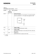
Introduction
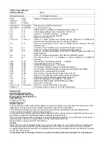
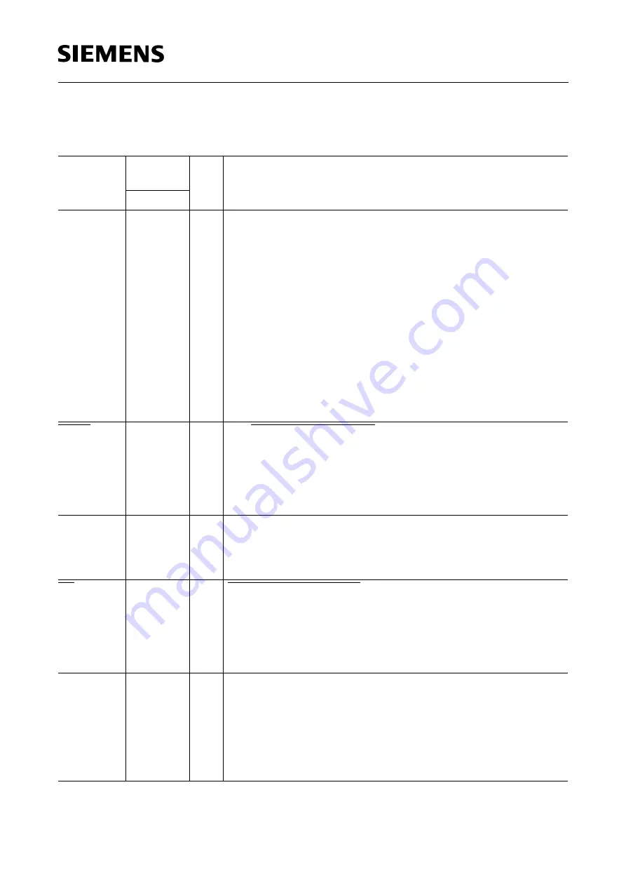
C541U
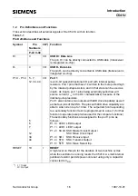
P2.0 - P2.7
24 - 31
I/O
Port 2
is an 8-bit quasi-bidirectional I/O port with internal pullup
resistors. Port 2 pins that have 1’s written to them are pulled high
by the internal pullup resistors, and in that state can be used as
inputs. As inputs, port 2 pins being externally pulled low will
source current (
I
IL
, in the DC characteristics) because of the
internal pullup resistors.
Port 2 emits the high-order address byte during fetches from
external program memory and during accesses to external data
memory that use 16-bit addresses (MOVX @DPTR). In this
application it uses strong internal pullup resistors when issuing
1’s. During accesses to external data memory that use 8-bit
addresses (MOVX @Ri), port 2 issues the contents of the P2
special function register.
PSEN
32
O
The Program Store Enable
output is a control signal that enables the external program
memory to the bus during external fetch operations. It is activated
every three oscillator periods except during external data memory
accesses. The signal remains high during internal program
execution.
ALE
33
O
The Address Latch enable
output is used for latching the address into external memory
during normal operation. It is activated every three oscillator
periods except during an external data memory access.
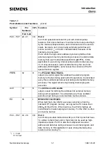
EA
35
I
External Access Enable
When held high, the C541U executes instructions from the
internal OTP program memory as long as the PC is less than
2000H for the C541U. When held low, the C541U fetches all
instructions from external program memory. For the C541U-L this
pin must be tied low.
P0.0 - P0.7
43 - 36
I/O
Port 0
is an 8-bit open-drain bidirectional I/O port. Port 0 pins that have
1’s written to them float, and in that state can be used as high-
impedance inputs. Port 0 is also the multiplexed low-order
address and data bus during accesses to external program and
data memory. In this application it uses strong internal pullup
resistors when issuing 1’s.
*) I = Input
O = Output
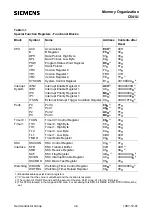
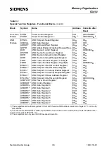
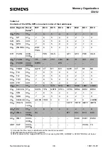
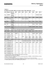
Table 1-1
Pin Definitions and Functions (cont’d)
Symbol
Pin
Numbers
I/O*) Function
P-LCC-44
Summary of Contents for C541U
Page 1: ... 8 LW 026 0LFURFRQWUROOHU 8VHU V 0DQXDO http www siem ens d Sem iconductor ...
Page 7: ......
Page 21: ...Semiconductor Group 2 6 1997 10 01 Fundamental Structure C541U ...
Page 37: ...Semiconductor Group 4 6 1997 10 01 External Bus Interface C541U ...
Page 133: ...Semiconductor Group 6 88 1999 04 01 On Chip Peripheral Components C541U ...
Page 163: ...Semiconductor Group 8 8 1997 10 01 Fail Safe Mechanisms C541U ...
Page 185: ...Semiconductor Group 10 14 1997 10 01 OTP Memory Operation C541U ...


