


Semiconductor Group
6-48
1999-04-01
On-Chip Peripheral Components
C541U
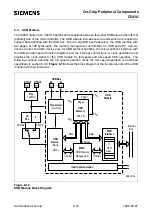
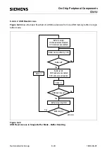
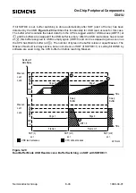
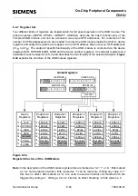
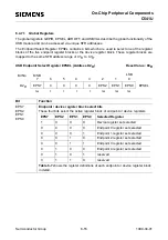
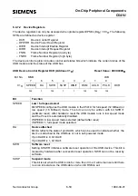
In general, three criteria for buffer switching are implemented in the USB module :
a) For sequential access, the address offset register ADROFF is automatically incremented after
each read or write action of the CPU. The address offset value (before incrementing)
represents the number of bytes stored in USB memory for a specific endpoint. If the address
offset value (after incrementing) reaches the value stored in endpoint length register EPLENn,
the currently active buffer is tagged full (USB read access - all bytes have been written by
CPU, CBF=1) or empty (USB write access - all bytes have been read by CPU, CBF=0).
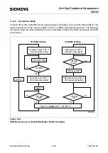
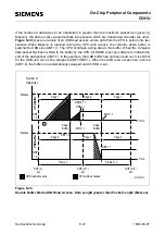
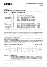
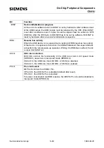
b) When Bit DONE, which is located in the endpoint buffer status register EPBSn, is set, software
buffer switching is initiated. This action is independent from the number of bytes which have
been handled by the CPU (possible in sequential access mode (INCE=1) and random access
mode (INCE=0)).
On CPU read accesses, the buffer is declared empty and bit CBF is cleared. If the buffer
assigned to the USB is full (UBF=1), the buffers are immediately swapped. In this case,
register EPLENn contains the number of received bytes.
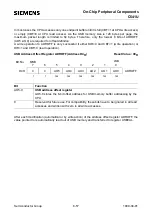
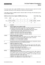
On CPU write accesses, two different cases must be distinguished. For random accesses, the
number of bytes of one packet is fixed by the value in register EPLENn and does not change.
For sequential accesses, the number of written bytes represents the packet size. In this case,
the actual value of register ADROFF is transferred to register EPLENn when bit DONE is set.
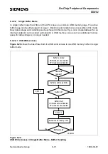
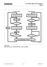
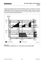
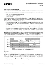
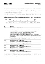
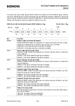
c) The third criteria for buffer switching is the automatic buffer switching on detection of SOF (see
figure 6-30). This feature can be individually enabled (SOFDE=1) or disabled (SOFDE=0) by
software selectively for each endpoint.
Summary of Contents for C541U
Page 1: ... 8 LW 026 0LFURFRQWUROOHU 8VHU V 0DQXDO http www siem ens d Sem iconductor ...
Page 7: ......
Page 21: ...Semiconductor Group 2 6 1997 10 01 Fundamental Structure C541U ...
Page 37: ...Semiconductor Group 4 6 1997 10 01 External Bus Interface C541U ...
Page 133: ...Semiconductor Group 6 88 1999 04 01 On Chip Peripheral Components C541U ...
Page 163: ...Semiconductor Group 8 8 1997 10 01 Fail Safe Mechanisms C541U ...
Page 185: ...Semiconductor Group 10 14 1997 10 01 OTP Memory Operation C541U ...


