Copyright © Siemens AG 2016. All rights reserved
157
ERTEC 200P-2 Manual
Technical data subject to change
Version 1.0
2.3.5 EMC (External Memory Controller)
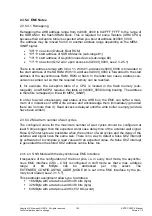
Modern SoC designs are often based on an “onchip” bus system, where various modules
are connected to. Within I DT / I IA the AMBA bus system of ARM is the most used one.
To allow masters on this bus system to access external memory devices, a functionality
is needed, which bridge from the internal AHB bus to external memory devices. This
functionality is provided with the External Memory Controller (EMC) module. The com-
plete description of the EMC please see following document 'EMC_....pdf' /36/ (see chap-
ter ):
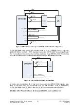
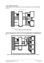
The EMC interface contains 2 separate memory controllers – SDRAM controller
(SDRAMC) and an asynchronous controller (ASYNCC) – for different devices like
SDRAM (including Mobile SDRAM) Memory
SRAM (including Flash EPROMs) Memory
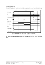
External devices, running a SRAM timing with additional READY signal
Burst Mode Flash ROM
It is connected to the system bus using an AHB slave interface with the following features
Supports AHB 2.0 lite protocol (No SPLIT, no RETRY)
Burst transactions are accepted at the AHB input side.
o
if the SDRAM controller is active, bursts of undefined length are split into
bursts of length 16.
o
if the asynchronous controller is active, any burst is split into single transfers
(exception of this rule: read access to Burst Flash ROM allows 16 beat burst,
read access to Page Mode ROM allows 16 beat burst).
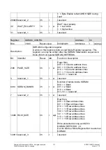
The EMC itself can be configured using the AHB slave interface
EMC comprises of 2 different controllers, one supporting the SDRAM Memory devices
(including Mobile SDRAM), the other supporting asynchronous SRAM timing in different
flavors, including Burst Flash ROM memory devices.
SDRAM-Controller features:
o
16/32 Bit databus width
o
PC133 SDRAM-compatible (125 MHz synchron is used in ERTEC 200P)
o
1 Bank with max. 256 MByte SDRAM (32 Bit databus)
o
SDRAM support for following parts:
CAS-Latency: 2 or 3 clocks
Bank-address bits (1/2/4 internal banks), realized via the lowest two bits
of the address bus MA(1:0)
8/9/10/11 bits column-address MA(13), MA(11:2)
max. 14 bits row-address MA(15:2)
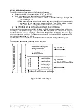
With 27 address lines (2 BANK, 14 ROW, 11 COL) it is possible to create 128M different
addresses. This 128M different addresses build up an address space of 512 MByte using
a 32 bit databus width, or 256 MByte using a 16 bit databus width. But the usable size is
limited by the EMC internal address decoder to a size of 256 Mbytes in total. SDRAMs
have a maximum of 4 internal banks. The SDRAM controller can open all 4 banks in
parallel. Those 4 banks are a quarter of the SDRAM address space at the AHB bus.
Asynchronous Controller features:
o
Can be set to 8/16/32-bit data bus width (for each chip select programmable)
o
4 chip selects
o
The timing for each chip select can be set individually
o
The response to ready signal can be set individually for each chip select

