Copyright © Siemens AG 2016. All rights reserved
270
ERTEC 200P-2 Manual
Technical data subject to change
Version 1.0
2.3.10.3.2
TIMER_TOP functionality
Block diagram:
TIMER_0
TIM_ MUX
Register
TIMER
EXT_EV_1_TIM_0
EXTERNAL_
INPUTS
Gate_Trig Control
Register
10
INT_GATE_TRIG_TIM_0
TIM_OUT_0
CLK_EN_TIM_0
EXT_GATE_TRIG_TIM_0
EXT_EV_2_TIM_0
Ext_Gate_Trig_
MUX Timer_0
Ext_Ev_1_
MUX Timer_0
Ext_Ev_2_
MUX Timer_0
...
TIMER_1... TIMER_5
TIMER_MUX_0
Clock
Divider
SW Event
Trigger
Register
TIMER_MUX_1-5
TIMER_TOP
Address
Predecoder
INT_EV_TIM_0
Output
MUX
Clock
Divider
Register
APB_IF
CLK_OUT
(1...10MHz)
TIM_OUT_1-5
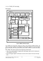
Figure 6: TIMER_TOP block diagram
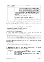
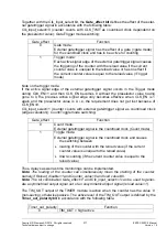
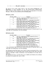
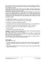
The TIMER_TOP submodule contains the wiring of the individual TIMER modules, the
Gate_Trig_Control registers, the multiplexer and timer MUX registers for the input signals
INT_GATE_TRIG_TIM, EXT_GATE_TRIG_TIM, EVENT1, EVENT2, and the clock divid-
er.
The TIMER_TOP module consists of the following functional units:
Gate_Trig_Control register for triggering SW gate/trigger signals and for releasing the
count pulses for the timers
SW event trigger register for storing the current counter values in the Int_Event regis-
ters


