Copyright © Siemens AG 2016. All rights reserved
422
ERTEC 200P-2 Manual
Technical data subject to change
Version 1.0
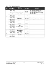
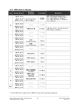
2.5 Detailed Address Mapping
Seg
Address-Range
Memory/
Peripheral
Size /Byte
Description
ARM926 subsystem
0
0x0
000_0000h
...
0x0
000_1FFFh
0x0
3FF_FFFFh
Boot ROM (8 KByte)
EMC (64 MByte)
8 KByte
64 MByte
MEM_SWAP parameter assignment:
00b: -> Boot ROM (0 - 8 KByte), imaged
F
01b: -> EMC SDRAM (0 - 64 MByte)
10b: -> EMC asyn memory (0 - 64 MByte)
11b: -> QVZ Error
0x0
000_0000h
...
0x0
003_FFFFh
ARM926 I-TCM
256 KByte
After ARM926 I-TCM activation (in the CP15
c9 register):
ARM 926 I-TCM (0 – 256 KByte physical. /
Step 64 KByte; not imaged);
0x0
404_0000h
...
0x0
7FF_FFFFh
Not used
< 64 MByte
0x0
800_0000h
...
0x0
803_FFFFh
ARM926 D-TCM
256 KByte
ARM 926 D-TCM (0 – 256 KByte physical. /
Step 64 KByte; not imaged);
0x0
804_0000h
...
0x0
FFF_FFFFh
Not used
< 128 MByte
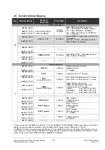
AHB peripherals
1
0x1
000_0000h
...
0x1
05F_FFFFh
ARM-ICU
6 MByte
ARM926 Interrupt Controller;
5 MByte physical;
2
0
* imaged;
0x1
060_0000h
...
0x1
07F_FFFFh
PN-IP
2 MByte
2 MByte physical; 2
0
* imaged;
0x1
080_0000h
...
0x1
09F_FFFFh
PerIF
(consistency buffer)
2 MByte
com. access:
128 KByte physical; 2
4
* imaged
appl. access:
64 KByte physical; 2
5
* imaged
0x1
0A0_0000h
...
0x1
0AF_FFFFh
GDMA
(register, JOB SRAM)
1 MByte
GDMA Register and internal
GDMA Job SRAM (Size: 4608 bytes)
1 MByte physical; 2
0
* imaged;
Register:
10A0_0000..10A0_00AF
JOB SRAM:
10A0_00B0..10A0_12AF
Not used:
10A0_12B0..10AF_FFFF
0x1
0D0_0000h
...
0x1
0DF_FFFFh
EMC register
1 MByte
EMC register;
1 MByte physical;
not imaged;
0x1
0E0_0000h
...
0x1
0EF_FFFFh
ETB11 memory
1 MByte
ETB11 memory;
8 KByte physical;
2
7
* imaged;
0x1
0F0_0000h
...
0x1
0FF_FFFFh
ETB11 register
1 MByte
ETB11 register;
512 byte physical;
2
11
* imaged;
0x1
100_0000h
...
0x1
10F_FFFFh
Not used
1 MByte
1 MByte physical;
not imaged;
0x1
110_0000h
Not used
239 MByte
14
After a reset, the boot ROM is at address 0. The first 64 MByte of EMC-SDRAM or EMC asyn memory (chip select
Bank0) can also be mapped to address 0 with the MEM_SWAP register in the SCRB (see 2.3.10.9.22).
15
ARM926 I-TCM can only be accessed internally from the ARM926 and not over the AHB. After activation, this ad-
dress range is no longer shown at the AHB. This range can also be shown at other addresses with alignment in seg-
ment 0, however not in the ARM926 D-TCM or ARM966 D-TCM area.


