Copyright © Siemens AG 2016. All rights reserved
457
ERTEC 200P-2 Manual
Technical data subject to change
Version
1.0
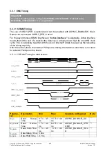
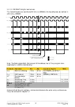
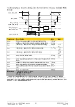
3.3.1.3.1 SDRAM Timing for read access
The Output-Signals are launched with CLK_O_SDRAMx, the Input-Signals are latched in
with CLK_I_SDRAM.
Note: The Bank signals BA0, BA1 are part of the address bus A. They are given here
separately for a better understanding.
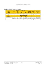
Parameter Description
Min
Max
depends on Register
Note
t
RCD
RAS to CAS delay
16
ns 32
ns EXTENDED_CONFIG.T
RCD
t
CAS
CAS Latency
16
ns
24
ns SDRAM_CONFIG.CL
t
RP
Row precharge
latency
24
ns
24
ns
t
DS
Data Setup Time
0.0
ns
CLK_I_SDRAM
t
DH
Data Hold Time
3.5
ns
CLK_I_SDRAM
Based
on
Tc = 8 ns (AHB Clock = 125 MHz);
Load-value for Timing = 20pF
Buffer Driverstrength = 12mA
IO-Voltage = 1.8V
Setup and hold times for address, command and data are the same as by a write access.
They can be found in chapter 7.2


