Copyright © Siemens AG 2016. All rights reserved
462
ERTEC 200P-2 Manual
Technical data subject to change
Version
1.0
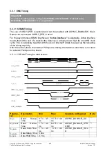
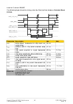
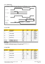
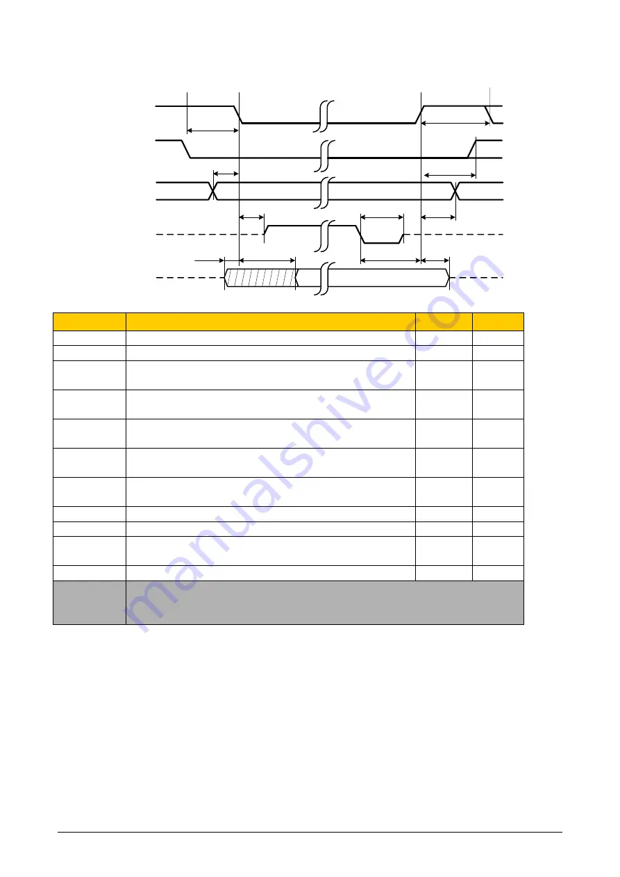
The following figure shows the timing, when the External Host initiates a
Common
Write
Access
:
t
WCS
t
ACS
t
CWH
t
WR
t
CAH
t
RAP
t
CRT
t
CDV
t
RTC
t
CDH
t
CDE
XHIF_XCS_M/R_I
XHIF_XWR_I
XHIF_A_I(19:0)
XHIF_SEG_I(2:0)
XHIF_XRDY_O /
XHIF_XRDY_OE
XHIF_D_I(31:0)
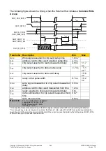
Parameter Description
Min
Max
t
WCS
Write signal asserted to chip selct setup time
1.6 ns
1)
t
ACS
address valid to chip select asserted setup time
2.1
ns
t
CRT
chip select asserted to ready deasserted delay
2.8
ns
11.7
ns
t
CDE
chip select asserted to data enable setup
-1.7 ns 1.1
ns
2)
t
CDV
chip select asserted to data valid delay
15.6
ns
t
RAP
ready active pulse width
6.1
ns
10.2
ns
t
CWH
write signal deasserted to chip select deasserted
delay
0.9
ns
t
CAH
address valid to chip select deasserted hold time
1.2 ns
t
RTC
ready asserted to chip select deasserted delay
0 ns
t
CDH
data valid/enabled to chip select deasserted hold
time
0 ns
2)
t
WR
write recovery time
8.8
ns
Based on
Tc = 8 ns (AHB Clock = 125 MHz);
Load-value for Timing = 20pF
Buffer Driverstrength = 9mA
IO-Voltage = 3,3V
1)
It is important to meet the setup timing of the Write signals; otherwise the XHIF module is driving the data bus
2)
t
CDE
may get any value, as long as it is assured, that there is 1 idle cycle (of the XHIF clock period) guaranteed be-
tween the end of the preceding access and the start of the current access (indicated by the falling edge of XHIF_XCS).
Within this idle cycle no access is allowed at all.

