Copyright © Siemens AG 2010. All rights reserved.
Page
53
ERTEC 400 Manual
Technical data subject to change
Version 1.2.2
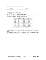
For the synchronous clock output of the SPI interface, the following frequencies are calculated according to the
assigned SPI registers:
50 MHz
SCLKOUT = -----------------------------
CPSDRV * (1+SCR)
The SPI parameters can assume the following values:
CPSDRV
From 2 to 254
SCR
From 0 to 255
This yields a frequency range of
•
769 Hz (CPSDRV = 254, SCR = 255) to
•
25 MHz (CPSDRV = 2, SCR = 0)
The SPI interface can also be used as a BOOT medium if, for example, functions from a serial EEPROM are to
be loaded to the ERTEC 400 and executed. The BOOT medium is selected by the BOOT[2:0] inputs during the
active reset phase. (See BOOT ROM description).
The BOOT loader then takes over setting of the SPI signal bins and loading of the program code. For BOOT
mode with SPI interface, the GPIO[22] is used as a chip select signal.
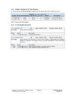
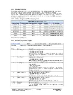
4.7.1
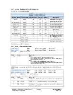
Address Assignment of SPI Register
The SPI registers are
16 bits in width
. For read/write access of the SPI registers to be meaningful, a 16-bit
access is required. However, a byte-by-byte write operation is not intercepted by the hardware.
SPI
(Base Address 0x4000_2200)
Register Name
Offset Address
Address Area
Access
Default
Description
SSPCR0
0x0000
2 bytes
R/W
0x0000
SSP control register 0
SSPCR1
0x0004
2 bytes
R/W
0x0000
SSP control register 1
SSPDR
0x0008
2 bytes
R/W
0x----
Rx/Tx FIFO data register
SSPSR
0x000C
2 bytes
R
0x0000
SSP status register
SSPCPSR
0x0010
2 bytes
R/W
0x0000
SSP clock prescale register
SSPIIR/SSPICR
0x0014
2 bytes
R/W
0x0000
Int identification register (read)
Interrupt clear register (write)
0x0018 - 0x003C
Reserved
0x0040 - 0x0090
Reserved for test purposes
0x0094 - 0x00FF
Reserved for future extension
Table 15: Overview of SPI Registers

