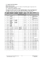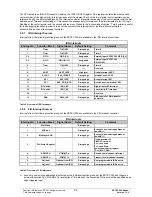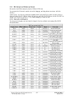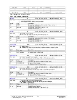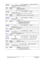
No.
Signal Name
I/O
Pull-
PIN
No.
Comment
PHY1 and PHY2
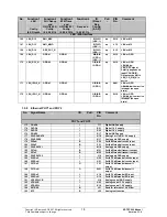
196 P1SDxN
I
F19
Port1 FX differential SD input
197 P1SDxP
I
G19
Port1 FX differential SD input
198 P1TDxN
O
C22
Port1 FX differential transmit
output
199 P1TDxP
O
C21
Port1 FX differential transmit
output
200 P1RDxN
I
E21
Port1 FX differential receive input
201 P1RDxP
I
E22
Port1 FX differential receive input
202 P1VSSATX2
I
K18
Analog port GND supply
203 P1TxP
B
J22
Port1 differential transmit output
204 P1TxN
B
J21
Port1 differential transmit output
205 P1VSSATX1
I
K17
Analog port GND supply
P1RxP
B
G21
206
Port1 differential receive input
207 P1RxN
B
G22
Port1 differential receive input
P1VSSARX
I
J17
Analog port GND supply
208
P1VDDARXTX
I
J19
Analog Port Tx/Rx 1.5 V supply
209
GND33ESD
I
H18
Analog test GND supply
210
211 VDD33ESD
I
F22
Analog test 3.3 V supply
212 DGND2
I
G17
Digital GND supply
213 DVDD2
I
H19
Digital 1.5 V supply
DVDD1
I
G18
Digital 1.5 V supply
214
DGND1
I
H21
Digital GND supply
215
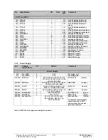
1.5.9 Power
Supply
No.
Voltage
Signal Name
I/O
PIN No.
Comment
Power Supply
216 PLL_AVDD
P
E12
PLL analog, 1.5 V
217 PLL_AGND
P
F13
PLL analog GND
218-238 VDD
Core
P
D6, D9, D12, D18, E5, E13, E18, F6,
F17, L4, R2, T21, U6, U8, U17, V4, V5,
V18, W13, W17, AA15
SV Core 1.5 V (21 pins)
239- 253
GND Core
P
A21, E6, E11, E17, F5, F7, F16, G6, L5,
T6, U16, V6, V11, V14, AA22
GND CORE (15 pins)
P
254-267 VDD
IO
SV IO 3.3 V (14 pins)
A2, A9, A10, A14, A18, B22, H1, N1,
W22, Y1, Y22, AB9, AB15, AB20
P
268-281 GND
IO
GND IO (14 pins)
A8, A12, A20, B1, B21, E10, F8, F15,
J1, T1, U5, U7, U15, V17
P
282-285 VDDQ
(PECL)
D21, D22, R19, V21
SV Q PECL 3.3 V (4 pins)
P
286-288 GND
(PECL)
F18, T18, T19
GND IO (PCI) (3 Pins)
Not Used Pins (16 Pins)
289-304
Not Used Pins
E19, F21, H17, J18, K21, K22,
M19, N19, N21, N22, P17, P18,
For improved heat dissipation
connect these pint to GND.
However, these pins can also
remain unconnected.
P19, R18, T22, V22
Table 1: ERTEC 200 Pin Assignment and Signal Description
Copyright © Siemens AG 2007. All rights reserved.
19
ERTEC 200 Manual
Technical data subject to change
Version 1.1.0

