5.1.2 JTAG
Clock
Supply
The clock supply for the JTAG interface is implemented using the
JTAG_CLK
pin. The frequency range is between 0
and 10 MHz. The boundary scan and the ICE macro cell of the ARM946E-S are enabled via the JTAG interface.
5.1.3
Clock Supply for PHYs and Ethernet MACs
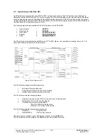
Both Ethernet MACs are connected to the integrated PHYs via the MII interface. The clock supply of the PHYs takes
place via the internal 25MHz clock
CLKP_A
. From this the PHYs generate the clock signals
RX_CLK
and
TX_CLK,
which are necessary for the Ethernet MACs.
Instead of the internal PHYs, external PHYs can also be connected to the ERTEC 200. In this case, the connections of
the MII interface of the MACs on the LBU interface must be made available.
The clock can be supplied to the external PHYs via the output pin
REF_CLK
(25MHz clock).
The output pin can be enabled/disabled with the configuration pin
CONFIG1
:
CONFIG1 = 0
Æ
Clock 25 MHz is enabled at output REF_CLK
CONFIG1 = 1
Æ
Clock 25 MHz is disabled at output REF_CLK
When external PHYs are used or to debug the Ethernet interfaces, the MII interface signals are made available at output
pins of the LBU interface. In both cases, the LBU interface is no longer available for connecting an external host
processor.
Selection of the MII interface signals on LBU pins takes place via configuration pins:
¾
CONFIG[6,5,2] = 111b
Æ
Connection of external PHYs
¾
CONFIG[6,5,2] = 011b
Æ
MII interface signals in debug mode
PHY0
(MII)
PHY1
(MII)
Ether-
net port
Buffer
MII
Ether-
net port
Buffer
MII
RX
_
C
L
K
TX_C
LK
RX
_
C
L
K
TX_C
LK
CLKP_A
(25 MHz)
MII Mode
ERTEC200
et
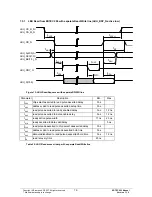
causes an internal reset of the entire circuitry including the clock system of the ERTEC 200 and saves the BOOT and
CONFIG pins to the internal registers. The hardware reset must be present steadily for
at least 35 µs
(see figure below).
Afterwards, the PLL powers up within t
Lock =
645 µs. In the ERTEC 200, the PowerOn reset phase is increased for this
time, and the clock system is not switched in until the end of the startup phase. Communication from the debugger via
the JTAG interface is not possible during this time. The following figure shows the power-up phase of the PLL after a
reset.
Figure 10: Clock Supply of Ethernet Interface
5.2 Reset Logic of the ERTEC 200
The reset logic resets the entire circuitry of the ERTEC 200.
The reset system of the ERTEC 200 is enabled by the following events:
•
Hardware reset via external
RESET_N
pin
•
Software
reset
via
XRES_SOFT
bit in the
RES_CTRL_REG
system control register
•
Watchdog reset via watchdog timer overflow
The triggering reset event can be read out in the
RES_STAT_REG
system control register.
5.2.1 PowerOn
reset
The external hardware reset circuitry is connected at the
RESET_N
pin of the ERTEC 200. Activating the hardware res
Copyright © Siemens AG 2007. All rights reserved.
65
ERTEC 200 Manual
Technical data subject to change
Version 1.1.0


