background image


7.5.4 

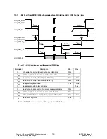
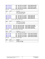
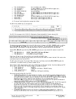
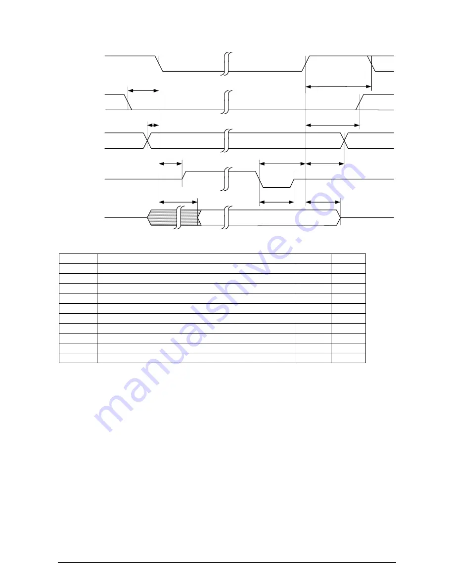
LBU Write to ERTEC 200 with common Read/Write line (LBU_RDY_N active low)


LBU_CS_R_N/ 
LBU_CS_M_N


LBU_WR_N


LBU_A(20:0)/ 
LBU_SEG(1:0)/ 
LBU_BE(1:0)_N


LBU_RDY


LBU_D(15:0)


t


WCS


t


ACS

t


CRE


t


CDV


t


CDH


t


CAH


t


CWH


t

RTC

t

RAP

t


WR


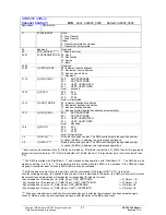
Figure 16: LBU-Write-Sequence with common RD/WR line 

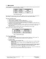
Parameter Description 

Min 

Max 

t

WCS

write signal asserted to chip select setup time 

2 ns

1


t

ACS

address valid to chip select asserted setup time 

0 ns 


t

CRE

chip select asserted to ready enabled delay 

5 ns 

12 ns 

t

CDV

chip select asserted to data valid delay 


40 ns 

t

RAP

ready active pulse width 

17 ns 

23 ns 

t

CWH

write signal deasserted to chip select deasserted hold time 

0 ns 


t

CAH

address valid to chip select deasserted hold time 

0 ns 


t

RTC

ready asserted to chip select deasserted delay 

0 ns 


t

CDH

data valid/enabled to chip select deasserted hold time 

0 ns 


t

WR

write recovery time 

25 ns 


Table 28: LBU Write access timing with common Read/Write line 

1

  The setup time 

t

WCS 

must be maintained under all circumstances; otherwise the LBU unit drives the ERTEC 200 

databus. 
 
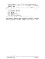
The ERTEC 200 has two LBU chip select inputs. One for access to the page configuration register (LBU_CS_R_N) and 
one to access to the ERTEC 200 memory address space (LBU_CS_M_N). Only one of these chip select signals may be 
active at a time and it is not allowed to change the chip select during the complete access.  

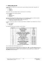
7.6  Host Interrupt Handling:


The ERTEC 200 generates 2 interrupt signals, LBU_IRQ0_N and LBU_IRQ1_N, to the external host. Both interrupts are 
generated in the IRT switch interrupt controller. Both signals are set by default to Low Active. However, they can also be 
assigned different parameters in the IRT switch. 
 
Mailbox handling between the ARM946E-S and an external host is possible via the IRT switch interrupt controller.   
An interrupt request from the ARM946E-S to the host processor is initiated by writing to the 

Activate_HP_Interrupt 

register.


An interrupt request from the host processor to the ARM946E-S is initiated by writing to the 

Activate_SP_Interrupt 

register.


Both registers can only be written to. Any value can be written.  


Copyright © Siemens AG 2007. All rights reserved.                  

82


ERTEC 200 Manual 

Technical data subject to change                                                                                                                                

Version 1.1.0


Summary of Contents for ERTEC200

Page 1: ...Copyright Siemens AG 2007 All rights reserved Page 1 ERTEC 200 Manual Technical data subject to change Version 1 1 0 RTEC 200 E nhanced Real Time Ethernet Controller E Manual ...

Page 2: ...d Copyright Siemens AG 2006 All rights reserved The reproduction transmission or use of this document or its contents is not permitted without express written authority Offenders will be liable for damages All rights including rights created by patent grant or registration of a utility model or design are reserved All product and system names are registered trademarks of their respective owner and...

Page 3: ... Structure of this Manual o Section 1 Overview of the architecture and the individual function groups of the ERTEC 200 o Section 2 ARM946E S processor systems o Section 3 Bus system of the ERTEC 200 o Section 4 I O of the ERTEC 200 o Section 5 General hardware functions o Section 6 External memory interface EMIF o Section 7 Local bus unit LBU o Section 8 DMA controller o Section 9 Ethernet PHYs o ...

Page 4: ...ressed in the documentation please contact your Siemens representative Please send your written questions comments and suggestions regarding the manual to the hotline via the e mail address indicated above In addition you can receive general information current product information FAQs and downloads pertaining to your application on the Internet at http www siemens com comdec Technical Contacts fo...

Page 5: ...Q 24 2 9 5 Nested Interrupt Structure 24 2 9 6 EOI End Of Interrupt 24 2 9 7 IRQ Interrupt Sources 25 2 9 8 FIQ Interrupt Sources 25 2 9 9 IRQ Interrupts as FIQ Interrupt Sources 26 2 9 10 Interrupt Control Register 26 2 9 11 ICU Register Description 27 2 10 ARM946E S Register 31 3 Bus System of the ERTEC 200 32 3 1 Multilayer AHB Communication Bus 32 3 1 1 AHB Arbiter 32 3 1 2 AHB Master Slave Co...

Page 6: ...Monitoring 67 5 3 3 EMIF Monitoring 67 5 4 Configuration Options on the ERTEC 200 67 6 External Memory Interface EMIF 69 6 1 Address Assignment of EMIF Registers 70 6 2 EMIF Register Description 70 7 Local Bus Unit LBU 74 7 1 Page Range Setting 76 7 2 Page Offset Setting 76 7 3 LBU Address Mapping 77 7 4 Page Control Setting 78 7 5 Host Access to the ERTEC200 78 7 5 1 LBU Read from ERTEC 200 with ...

Page 7: ...erface 95 11 3 JTAG Interface 95 11 4 Debugging via UART 95 12 Miscellaneous 96 12 1 Acronyms Glossary 96 12 2 References 97 Copyright Siemens AG 2007 All rights reserved Page 7 ERTEC 200 Manual Technical data subject to change Version 1 1 0 ...

Page 8: ...able 10 Overview of Timer Registers 40 Table 11 Overview of F Timer Registers 44 Table 12 Overview of WD Registers 46 Table 13 Baud Rates for UART at FUARTCLK 50 MHz 49 Table 14 Overview of UART Registers 49 Table 15 Overview of SPI Registers 55 Table 16 Overview of System Control Registers 59 Table 17 Overview of ERTEC 200 Clocks 64 Table 18 Configurations for ERTEC 200 68 Table 19 Overview of EM...

Page 9: ...e ERTEC 200 is a high performance Ethernet controller with the following integrated function groups High performance ARM 946 processor with D cache I cache D TCM memory Multilayer AHB bus master slave with AHB arbiter IRT switch with 64 Kbyte communication RAM 2 Ethernet channels with integrated PHYs Local Bus Unit LBU for connecting an external host processor with boot capability SDRAM controller...

Page 10: ...st Multi Layer AHB 50 MHz 32Bit Memory Controller EMIF Slave Input stage MUX Arb MUX Arb MUX Arb 4 Reset System Control Clock Unit F_CLK 48 Local Bus Unit 16 Bit LBU Master Input stage MUX ERTEC200 MC PLL Signals PHY Port 1 PHY Port 2 ARM946ES with I Cache 8kByte D Cache 4kByte D TCM 4kByte Master 7 BS TAP JTAG Debug AHB Wrapper Master MC Bus 50MHz 32 Bit Slave Input stage ARM Interrupt Controller...

Page 11: ...or the ERTEC 200 can be found in the following documents 10 Soldering instructions for lead based block 11 Soldering instructions for lead free block 12 Code description for soldering When working with modules always take precautionary measures against electrostatic charge ESD Electrostatic Sensitive Devices Copyright Siemens AG 2007 All rights reserved Page 11 ERTEC 200 Manual Technical data subj...

Page 12: ...3 P2 SPEED 100LED_N TX FX P2 SPEED 10LED_N B O O I up B19 GPIO or PHY LED O 5 GPIO4 P1 LINK LED_N B O I up A19 GPIO or PHY LED O 6 GPIO5 P2 LINK LED_N B O I up D16 GPIO or PHY LED O 7 GPIO6 P1 RX LED_N P1 TX LED_N P1 ACTIVE LED_N B O O O I up B18 GPIO or PHY LED O 8 GPIO7 P2 RX LED_N P2 TX LED_N P2 ACTIVE LED_N B O O O I up D15 GPIO or PHY LED O 9 GPIO8 UART TXD B O I up B17 GPIO or UART O 10 GPIO...

Page 13: ... or DEBUG I 1 For an IRT application pin GPIO25 is default parameterized as alternate function1 TGEN_OUT1_N A synchronous clock is issued at this pin During the certification process of a PROFINET IO DEVICE with IRT functionality this pin has to be accessible from outside mandatory Different GPIO s are used on the Evaluation Board EB200 See Dokument 14 Table 6 1 5 2 JTAG and Debug No Signal Name I...

Page 14: ... up E7 Direction signal for external driver or scan clock Scan mode ERTEC 200 boot mode external PD may be necessary 52 OE_DRIVER_N O O D8 Enable signal for external driver or scan clock Scan mode 53 A0 O O B4 Address bit 0 SDRAM Bank address 0 54 A1 O O A3 Address bit 1 SDRAM Bank address 1 55 A2 O O B3 Address bit 2 SDRAM Address 0 56 A3 O O B2 Address bit 3 SDRAM Address 1 57 A4 O O D4 Address ...

Page 15: ...sary 76 A23 CONFIG6 B I up H4 Address bit 23 ERTEC 200 system configuration external PD may be necessary 77 D0 B I up M2 Data bit 0 78 D1 B I up N2 Data bit 1 79 D2 B I up P1 Data bit 2 80 D3 B I up P2 Data bit 3 81 D4 B I up R1 Data bit 4 82 D5 B I up T2 Data bit 5 83 D6 B I up U1 Data bit 6 84 D7 B I up U2 Data bit 7 85 D8 B I up V2 Data bit 8 86 D9 B I up W1 Data bit 9 87 D10 B I up W2 Data bit...

Page 16: ...PIN No Comment LBU MII Interface ETM Trace Interface 125 LBU_A0 RXD_P10 ETMEXTOUT I O O I ETM I up AB3 LBU or MII or ETM 126 LBU_A1 RXD_P11 ETMEXTIN1 I O I I ETM I up AA4 LBU or MII or ETM 127 LBU_A2 RXD_P12 TRACEPKT7 I O O I ETM I up AA5 LBU or MII or ETM 128 LBU_A3 RXD_P13 TRACEPKT6 I O O I ETM I up AB5 LBU or MII or ETM 129 LBU_A4 CRS_P1 TRACEPKT5 I O O I ETM I up AA6 LBU or MII or ETM 130 LBU_...

Page 17: ...ow Active CONFIG 5 1 150 LBU_CS_R_ N GPIO39 GPIO39 I B B B GPIO I up AB12 LBU or GPIO LBU Mode CS for paging configuration register 151 LBU_CS_M_ N GPIO40 GPIO40 I B B B GPIO I up U14 LBU or GPIO LBU Mode CS for ERTEC 200 resources 152 LBU_BE0_N RX_CLK_P1 I O I I up AB14 LBU or MII 153 LBU_BE1_N RX_CLK_P2 I O I I up AA13 LBU or MII 154 LBU_D0 TXD_P10 B O I O LBU I up AA14 LBU or MII 155 LBU_D1 TXD...

Page 18: ...tal GND supply 174 DVDD4 I R21 Digital 1 5 V supply 175 DVDD3 I R22 Digital 1 5 V supply 176 DGND3 I R17 Digital GND supply 177 P2VDDARXTX I N18 Analog Port Tx Rx 1 5 V supply 178 P2VSSARX I N17 Analog port GND supply 179 P2RxN B P22 Port2 differential receive input 180 P2RxP B P21 Port2 differential receive input 181 P2VSSATX1 I M18 Analog port GND supply 182 P2TxN B M21 Port2 differential transm...

Page 19: ... 5 V supply DVDD1 I G18 Digital 1 5 V supply 214 DGND1 I H21 Digital GND supply 215 1 5 9 Power Supply No Voltage Signal Name I O PIN No Comment Power Supply 216 PLL_AVDD P E12 PLL analog 1 5 V 217 PLL_AGND P F13 PLL analog GND 218 238 VDD Core P D6 D9 D12 D18 E5 E13 E18 F6 F17 L4 R2 T21 U6 U8 U17 V4 V5 V18 W13 W17 AA15 SV Core 1 5 V 21 pins 239 253 GND Core P A21 E6 E11 E17 F5 F7 F16 G6 L5 T6 U16...

Page 20: ...le of IO Function B O O I I Æ Function 0 Bidirectional Function 1 Output Function 2 Output Function 3 Input I IO Function during RESET Input For LBU PHY Debug or ETM Trace Interface the IO function is active during Reset which is selected with the pins CONFIG 6 5 2 Default the Function 3 ETM Trace GPIO 44 32 is set with internal Pullup and Pulldown resistors Unusual feature ETM outputs are switche...

Page 21: ...f the processor In addition to the processor core the system contains one data cache one instruction cache a memory protection unit MPU a system control coprocessor and a tightly coupled memory The processor system has an interface to the integrated AHB bus Figure 3 Structure of ARM946E S Processor System Copyright Siemens AG 2007 All rights reserved 21 ERTEC 200 Manual Technical data subject to c...

Page 22: ... instruction cache This mechanism can only be applied at the segment level with the ARM946E S Both caches are locked after a reset These caches can only be enabled if the Memory Protection Unit is also enabled The I cache can be enabled by setting Bit 12 of the CP15 control register The D cache can be enabled by setting Bit 2 of the CP15 control register Access to this area is blocked if the cache...

Page 23: ...bus and address bus each have a width of 32 bits For more information about the bus interface and write buffer and about the different transfer types refer to Document 1 Section 6 2 8 ARM946E S Embedded Trace Macrocell ETM9 An ETM9 module is connected at the ARM946E S This module permits debugging support for data and instruction traces in the ERTEC 200 The module contains all signals required by ...

Page 24: ...ed by the ARM946 CPU and an entry is made in the in service request register ISR the corresponding bit is reset in the IRREG register Each bit that is set in the IRREG register can be deleted via software For this purpose the number of the bit to be reset in the IRCLVEC register is transferred to the interrupt controller 2 9 4 Software Interrupts for IRQ Every IRQ interrupt request can be triggere...

Page 25: ...Y 0 1 10 SPI SSP_INTR Rising edge Group interrupt SPI 11 SPI SSP_ROR_INTR Rising edge Receive overrun interrupt SPI 12 IRT switch IRQ0_SP Rising edge High priority IRT interrupt 13 IRT switch IRQ1_SP Rising edge Low priority IRT interrupt 14 Reserved 15 DMA DMA_INT Rising edge DMA controller DMA transfer complete Table 2 Overview of IRQ Interrupts 2 9 8 FIQ Interrupt Sources Interrupts from the fo...

Page 26: ...00001 Mask for all interrupts IRQEND 0x0024 4 bytes W 0x End of IRQ interrupt FIQEND 0x0028 4 bytes W 0x End of FIQ interrupt FIQPR0 0x002C 4 bytes R W 0x00000007 FIQ priority register on input FIQ0 of the FIQ interrupt controller FIQPR1 0x0030 4 bytes R W 0x00000007 FIQ priority register on input FIQ1 of the FIQ interrupt controller FIQPR2 0x0034 4 bytes R W 0x00000007 FIQ priority register on in...

Page 27: ...Description 3 0 LOCKPRIO Binary code of lock priority 7 LOCKENABLE 0 Lock inactive 1 Lock active FIQ1SREG R W Addr 0x5000_000C Default 0x0000_0000 Description Fast interrupt request 1 select register Declaration of an IRQ input as FIQ6 input FIQ6 on FIQ interrupt controller Bit No Name Description 3 0 FIQ1SREG Number of the input to be selected binary code 7 FIQ1SENABLE 0 Ignore FIQ declaration 0 ...

Page 28: ...on End of interrupt IRQ Communicates to the IRQ interrupt controller the completion of the interrupt service routine associated with the current request Bit No Name Description Not used FIQEND W Addr 0x5000_0028 Default Description End of interrupt FIQ Communicates to the FIQ interrupt controller the completion of the interrupt service routine associated with the fast interrupt request Bit No Name...

Page 29: ...r Enable disable of interrupt inputs Bit No Name Description 15 0 MASKREG Interrupt input 0 to 15 0 Interrupt input enabled 1 Interrupt input disabled ISREG R Addr 0x5000_0060 Default 0x0000_0000 Description In service register Indication of the interrupt requests confirmed by the CPU Bit No Name Description 15 0 ISREG Interrupt input 0 to 15 0 Interrupt request not confirmed 1 Interrupt request h...

Page 30: ...t 1 Set interrupt request PRIOREG 0 R W Addr 0x5000_0070 Default 0x0000_000F PRIOREG 15 R W Addr 0x5000_00AC Default 0x0000_000F Description Priority register Specification of priority of an interrupt request at the associated input Bit No Name Description 3 0 PRIOREG Binary code of the priority Copyright Siemens AG 2007 All rights reserved 30 ERTEC 200 Manual Technical data subject to change Vers...

Page 31: ...r 2 7 W Cache operation register 8 xxx Undefined 9 W R Cache lockdown register 2 10 xxx Undefined 11 xxx Undefined 12 xxx Undefined 13 W R Trace process ID register 14 xxx Undefined 15 W R RAM TAG BIST test register 1 Test state register 1 Cache debug index register 1 Trace control register Table 5 CP15 Registers Overview 1 Registers contain multiple information entries that are selected by the op...

Page 32: ...uences on the multilayer AHB bus The round robin arbitration procedure prevents mutual blocking of the AHB master over a long period on the multilayer AHB bus With fixed priority assignment the ARM has the highest priority assignment followed by IRT DMA and LBU with the lowest priority 3 1 2 AHB Master Slave Coupling The table below shows which AHB masters can communicate with which AHB slaves AHB...

Page 33: ... decoded out memory or register areas trigger an FIQ1 interrupt Access by a generated Ready signal from the APB address decoder is closed Write accesses do not affect the system Read accesses supply undefined data 4 1 BOOT ROM The ERTEC 200 is implemented with a BOOT ROM whose integrated opcode enables software to be downloaded from an external storage medium Various routines are available for the...

Page 34: ...Data Flash e g AT45DB011B GPIO 23 1 Æ SPI compatible EEPROM e g AT25HP256 The GPIO 22 GPIO cable is used as the chip select for the SDI memory The serial protocols by Motorola Texas Instruments and NSC are supported in principle 4 1 3 Booting via UART Boot mode via UART uses a bootstrap method that first downloads to the ERTEC200 a routine for operating the serial interface which then performs the...

Page 35: ...t the IRQ interrupt controller of the ARM946 The polarity of the GPIO interrupts can be specified with the GPIO_POLSEL register see GPIO register description The following figure shows the structure of a GPIO 31 0 pin as a normal I O function or as an alternative function GPIO i GPIO IN GPIO OUT i Alternate function 1 2 3 if input Alternate function 1 2 3 if output GPIO IOCTRL i GPIO_PORT MODE_L _...

Page 36: ...Register Description GPIO_IOCTRL W R Addr 0x4000_2500 Default 0xFFFF_FFFF Description Configuration register for General Purpose IO 31 0 Bit No Name Description 31 0 GPIO_IOCTRL 31 0 0 GPIOx is output 1 GPIOx is input x Bit 0 31 GPIO_ OUT W R Addr 0x4000_2504 Default 0x0000_0000 Description Output register for General Purpose IO 31 0 Bit No Name Description 31 0 GPIO_OUT 31 0 0 GPIO outputx 0 1 GP...

Page 37: ... 27 26 GPIO29_PORT_MODE Port GPIO 29 29 28 GPIO30_PORT_MODE Port GPIO 30 31 30 GPIO31_PORT_MODE Port GPIO 31 GPIO_POLSEL W R Addr 0x4000_2514 Default 0x0000_0000 Description Interrupt polarity for GPIO interrupts 31 30 1 0 Bit No Name Description 31 4 Reserved Reserved 3 POLSEL GPIO31 0 GPIO31 is not inverted to ICU IRQ5 1 GPIO31 is inverted to ICU IRQ5 2 POLSEL GPIO30 0 GPIO30 is not inverted to ...

Page 38: ...timers 0 1 are deactivated after reset The timers are enabled by setting the RUN XStop bit in the status control register of the respective timer The timer then counts downwards from its loaded 32 bit starting value When the timer value reaches 0 a timer interrupt is generated The interrupt can then be evaluated by the IRQ interrupt controller Depending on the reload mode the two timers behave as ...

Page 39: ...for data consistency in the user software when reading out the 64 bit timer 4 3 2 Timer 2 Timer2 has the following functionality 16 bit count register Fixed 50 MHz input clock Up counter 16 bit reload value Start stop function Interrupt when counter state 0 is reached Different function modes can be assigned one shot cycle and retrigger mode Timer 2 can be used for general monitoring functions Tim...

Page 40: ...figuration and control bits for Timer No 0 Bit No Name Description 0 Run xStop Stop start of timer 0 Timer is stopped 1 Timer is running Note If this bit 0 the timer interrupt is inactive 0 and the status bit Bit 5 is reset 0 1 Load Trigger Load the timer with the reload register value 0 Not relevant 1 Timer is loaded with the value of the reload register irrespective of Bit 0 Run xStop While this...

Page 41: ...aded RELD0 R W Addr 0x4000_2008 Default 0x0000_0000 RELD1 R W Addr 0x4000_200C Default 0x0000_0000 Description Reload registers 0 to 1 Reload value for timers 0 to 1 Bit No Name Description 31 0 Reload 31 0 Reload value of timer CTRL_PREDIV R W Addr 0x4000_2010 Default 0x0000_0000 Description Control register for the two prescalers Bit No Name Description 0 Run xStop_V0 Stop start of prescaler 0 0...

Page 42: ...Timer 2 Control Register Bit No Name Description 31 19 Reserved Reserved 18 Timer_Mode 0 Cyclic 1 Retrigger via UART_RXD signal for RXD at log 0 17 OneShot_Mode 0 Cycle timer Timer 2 is loaded with 0000h when timer value reload value and continues to run 1 OneShot Timer Timer 2 stops when timer value reload value 16 Run xStop 0 Stop Timer 2 reset Timer 2 deactivate INT 1 Start Timer 2 15 0 Reload ...

Page 43: ...don t care to the F counter register FCOUNT_RES The next count pulse sets the counter to 0xFFFF FFFF and the counter is decremented at each additional count pulse The FCOUNT_RES register is cleared again at the next clock cycle The count value can be read out by a 32 bit read access While an 8 bit or 16 bit read access is possible it is not useful because it can result in an inconsistency in the r...

Page 44: ...OUNTER VAL R Addr 0x4000_2700 Default 0x0000_0000 Description Timer value of F counter Bit No Name Description 31 0 F CNT VAL 31 0 Timer value of F timer F COUNTER RES W Addr 0x4000_2704 Default 0x0000_0000 Description Reset register for F counters A reset of the F counter is performed only if 0xXXXX 55AAh is entered in this register Resets are thus possible via 16 bit and 32 bit accesses Bit No N...

Page 45: ... is read bits 35 4 are read out The status of the two watchdog timers can be read out in the CTRL STATUS register 4 5 3 Watchdog Interrupt The WDINT interrupt of the watchdog is routed to the FIQ interrupt controller The FIQ0 interrupt is only active High if watchdog timer 0 is in RUN mode and watchdog timer 0 has reached zero The exception to this is a load operation with reload value 0 4 5 4 WDO...

Page 46: ...guration and control bits for the watchdog Bit No Name Description 0 Run xStop_V0 Enable disable watchdog counter 0 0 Watchdog counter 0 disabled 1 Watchdog counter 0 enabled Note If this bit 0 the WDOUT0_n output of the ERTEC 200 is active 0 the interrupt of the watchdog WDINT is 0 and the status bit of counter 0 Bit 3 is 0 1 Run xStop_Z1 Enable disable watchdog counter 1 0 Watchdog counter 1 dis...

Page 47: ...ter 1 Bit No Name Description 15 0 Reload1 19 4 Reload value for bits 19 4 of watchdog counter 1 31 16 Key bits Key bits for writing to this register read 0 If bits 31 16 9876h writing of bits 0 15 of this register has an effect otherwise no effect RELD1_HIGH R W Addr 0x4000_2110 Default 0x0000_FFFF Description Reload register 1_High Reload value for bits 35 20 of watchdog counter 1 Bit No Name De...

Page 48: ... Block Diagram of UART The UARTs differ from standard UART 16C550 as follows Receive FIFO trigger level is set permanently to 8 bytes Receive errors are stored in the FIFO Receive errors do not generate an interrupt The internal register address mapping and the register bit functions are different The following standard UART 16C550 features are not supported 1 5 Stop bits Forcing stick parity func...

Page 49: ... BOOT medium if for example functions C 200 and executed The BOOT medium is selected by the BOOT loader then takes over setting of the UART signal pins and loadin nality is also used s not utilize the UART it can also be used as a debugging in Address Assignment of UART Registers registers are 8 bits in width UART Start 0x4000_2300 Register Name Offset Address Address Area Access Default Descripti...

Page 50: ... UART receive error clear register write Bit No Name Description 7 0 Write Framing errors parity errors break errors and overrun errors are deleted 0 FE Read Framing error 1 Received character does not have a valid stop bit 1 PE Read Parity error 1 Parity of received character does not match the assigned parity in the UARTLCR_H register Bit 2 2 BE Read Break error 1 A break was detected A break me...

Page 51: ...rame 00 5 bit data 01 6 bit data 10 7 bit data 11 8 bit data 7 Reserved Value is undefined UARTLCR_M R W Addr 0x4000_230C Default 0x00 Description UART line control register middle byte baud rate high byte bits 15 8 Bit No Name Description 7 0 BAUD DIVMS Baud rate divisor high byte UARTLCR_L R W Addr 0x4000_2310 Default 0x00 Description UART line control register low byte baud rate low byte bits 7...

Page 52: ...l of UART input CTS 1 DSR Data Set Ready This bit is the inverse signal of UART input DSR 2 DCD Data Carrier Detect This bit is the inverse signal of UART input DCD 3 BUSY UART Busy The bit is set if send data are in progress or if the Transmit FIFO is not empty 4 RXFE Receive FIFO Empty 1 if FIFO is disabled and Receive holding register is empty FIFO is disabled and Receive FIFO buffer is empty 5...

Page 53: ...This bit is set if UARTRTINTR is active 7 4 Read Reserved Value is undefined 7 0 Write Writing to this register deletes the MIS bit irrespective of the value written UARTILPR R W Addr 0x4000_2320 Default 0x00 Description UART IrDA low power counter registers not supported in the ERTEC 200 Bit No Name Description 7 0 ILPDVSR 8 bit low power divisor value NOTE The low power divisor is calculated acc...

Page 54: ...plemented as ARM Prime CellTM PL021 Macros For a detailed description refer to 6 The figure below shows the structure of the SPI macro Figure 8 Block Diagram of SPI The SPI interface supports the following modes Motorola SPI compatible mode Texas Instruments synchronous serial interface National Semiconductor microwire interface The SPI interface has the following features Separate send and receiv...

Page 55: ...ed as a chip select signal 4 7 1 Address Assignment of SPI Register The SPI registers are 16 bits in width Reading or writing the SPI register is useful only in 16 bit access byte by byte write operation is not intercepted by the hardware SPI Base Address 0x4000_2200 Register Name Offset Address Address Area Access Default Description SSPCR0 0x0000 2 bytes R W 0x0000 SSP control register 0 SSPCR1 ...

Page 56: ... Register SSPCR1 R W Addr 0x4000_2204 Default 0x0000 Description Control register 1 Configuration frame format and baud rate for SPI Bit No Name Description 0 RIE Receive FIFO interrupt enable 0 Receive FIFO half full or more interrupt SSPRXINTR is disabled 1 Receive FIFO half full or more interrupt SSPRXINTR is enabled 1 TIE Transmit FIFO interrupt enable 0 Transmit FIFO half full or less interru...

Page 57: ...t FIFO is full 1 Transmit FIFO is not full 2 RNE Receive FIFO not empty 0 Receive FIFO is empty 1 Receive FIFO is not empty 3 RFF Receive FIFO full 0 Receive FIFO is not full 1 Receive FIFO is full 4 BSY SPI busy flag 0 SPI is 1 SPI is sending and or receiving a frame or the Transmit FIFO is not empty 15 5 Reserved Read Value is undefined Write Should always be written with zero SSPCPSR R W Addr 0...

Page 58: ...Boot Pins Boot mode pins Boot 3 0 SER_CFG_REG 0x0008 4 bytes R Config Pins ERTEC 200 config pins Config 6 1 RES_CTRL_REG 0x000C 4 bytes W R 0x00000004 Control register for reset of ERTEC 200 RES_STAT_REG 0x0010 4 bytes R 0x00000004 Status register for reset of ERTEC 200 PLL_STAT_REG 0x0014 4 bytes R W 0x00070005 Status register for PLL FIQ3 QVZ_AHB_ADR 0x0028 4 bytes R 0x00000000 Address of incorr...

Page 59: ...rol register for reset of ERTEC 200 Bit No Name Description 31 13 Reserved Reserved 12 3 PULSE_DUR Pulse duration of SW or watchdog reset TRES_PULSE 8 x n 8 x TCLK TCLK APB clock period 1 50 MHz 20 ns n Value of PULSE_DUR 0 1023 The integrated PHYs require a reset duration of 100µs This requires the setting n 625 2 EN_WD_SOFT_ RES_IRTE 0 The IRTE switch controller is not reset for the watchdog sof...

Page 60: ...ccessible 2 INT_LOCK_STATE Interrupt lock state INT_LOCK_STATE 0 Interrupt request is inactive 1 Interrupt request is active This bit indicates whether the PLL was in unlocked state latching Read write accessible 1 PLL_INPUT_CLK_LO SS Loss Monitoring status of PLL input clock 1 PLL input clock not detected 0 PLL input clock available This bit indicates the current monitoring status of the PLL inpu...

Page 61: ...served Reserved 1 0 MEM_SWAP Selection of memory in Segment 0 on the AHB 00 Boot ROM starting with Addr 0h 01 EMIF SDRAM starting at Adr 0h 10 EMIF Standard Memory starting at Adr 0h 11 No memory starting from Addr 0h Locked I Cache can be placed on Addr 0h M_LOCK_CTRL R W Addr 0x4000_264C Default 0x0000_0000 Description AHB master lock enable Master selective enable of AHB lock functionality Bit ...

Page 62: ...on this bit 8 0 SYSOPT 8 0 ETM Option SYSOPT 8 0 Indicates the implemented ETM options Default value 139H ARM9_WE R W Addr 0x4000_2654 Default 0x0000_0000 Description Write access register for the ARM9_CTRL register Bit No Name Description 31 1 Reserved 0 WE_ARM9_CTRL Write enable for ARM9_CTL register 1 ARM9_CTRL can be write accessed 0 ARM9_CTRL is read only ERTEC 200_TAG R W Addr 0x4000_2658 De...

Page 63: ...ASE FX interface is enabled only meaningfule when P1_PHY_Mode 010 or 011 0 The 100BASE FX interface is disabled 0 P1_PHY_ENB 0 PHY1 disabled Powerdown Mode 2 1 PHY1 enabled 1 2 PHY_ STATUS R Addr 0x4000_2660 Default 0x0000_0000 Description Status of PHY1 and PHY2 Bit No Name Description 31 9 Reserved 8 P2_PWRUPRST 0 PHY2 in Powerdown mode or internal reset is still active 1 PHY2 is ready for opera...

Page 64: ...KP_A The input clock is divided down by a factor of 12 5 MHz and fed into the PLL The PLL generates a clock of 300 MHz which supplies the following clock generator This generates all system clock required for the ERTEC 200 The following figure shows the generation of the ERTEC 200 clocks Divider 1 2 REF_CLK 25 MHz CONFIG1 APLL PLL_IN 12 5 MHz PLL_OUT 300 MHz CONFIG4 CONFIG3 MUX MUX MUX SCANMODE CL...

Page 65: ...ins CONFIG 6 5 2 111b Æ Connection of external PHYs CONFIG 6 5 2 011b Æ MII interface signals in debug mode PHY0 MII PHY1 MII Ether net port Buffer MII Ether net port Buffer MII RX_CLK TX_CLK RX_CLK TX_CLK CLKP_A 25 MHz MII Mode ERTEC200 et causes an internal reset of the entire circuitry including the clock system of the ERTEC 200 and saves the BOOT and CONFIG pins to the internal registers The h...

Page 66: ...The watchdog reset involves ring is based on a time setting in the watchdog timer This is started when the r at a specified reload value prevents the watchdog reset from being trig atchdog reset is enabled after the timer expires if the watchdog function is acti dog reset is controlled in the ERTEC 200 by means of assignable pulse str complete ERTEC 200 circuit As is the case with the hardw RES_ST...

Page 67: ..._Bank_3_Config configuration registers If one of the four memory areas that are selected via the CS_PER0_N to CS_PER3_N chip select outputs is addressed the memory controller of the ERTEC 200 waits for the RDY_PER_N input signal The monitoring duration is set in the ASYNC_WAIT_CYCLE_CONFIG EMIF register and is active if timeout monitoring Bit 7 is set in the EXTENDED_CONFIG EMIF register The speci...

Page 68: ...N is high active 0 0 LBU On LBU_POL_RDY LBU_RDY_N is low active 0 1 1 LBU off GPIO44 32 on int PHYs On ext MII PHY debugging ETM9 Off 1 0 1 LBU off GPIO44 32 on int PHYs On ext MII Off ETM9 On 1 1 1 Reserved 0 0 ARM clock 50 MHz 0 1 ARM clock 100 MHz 1 0 ARM clock 150 MHz 1 1 Reserved Table 18 Configurations for ERTEC 200 Copyright Siemens AG 2007 All rights reserved 68 ERTEC 200 Manual Technical ...

Page 69: ...bytes of SDRAM for 32 bit data bus width Supports various SDRAMs with the following properties o CAS latency 2 or 3 clock cycles o 1 2 4 internal banks can be addressed A1 0 o 8 9 10 11 bits column address A13 11 2 o Maximum of 13 row addresses A14 2 SDRAMS with a maximum of 4 banks are supported The SDRAM controller can keep all 4 banks open simultaneously In terms of addresses these four banks c...

Page 70: ...iming data bus width for access via async interface CS_PER2_N Async_BANK3_ Config 0x001C 4 bytes W R 0x3FFFFFF2 Timing data bus width for access via async interface CS_PER3_N Extended_Config 0x0020 4 bytes W R 0x03030000 Setting of additional functionalities Table 19 Overview of EMIF Registers 6 2 EMIF Register Description Revision Code and Status R Addr 0x7000_0000 Default 0x0000_0100 Description...

Page 71: ...ess lines 100 111 Reserved Attention Writing to SDRAM_Bank_Config 15 7 executes the Mode Register Set command on the SDRAM if Bit 29 init_done is set in the SDRAM_Refresh_Control register i e the SDRAM power up sequence has been executed SDRAM Refresh Control W R Addr 0x7000_000C Default 0x0000_0190 Description Setting of refresh rate indication for timeout Bit No Name Description 31 Reserved Rese...

Page 72: ...te signal 25 20 W_STROBE Write strobe duration cycles w_strobe 1 AHB clock cycles between falling and rising edges of the write signal 19 17 W_HOLD Write strobe hold cycles w_hold 1 AHB clock cycles between rising edge of the write signal and change of address data and chip select 16 13 R_SU Read strobe setup cycles r_su 1 AHB clock cycles between valid address and chip select and falling edge of ...

Page 73: ... for asynchronous accesses disabled 1 Timeout watchdog for asynchronous accesses enabled After the watchdog expires 256 AHB clock cycles an interrupt is triggered Setting Bit 7 to 0 deletes interrupt source 6 0 Reserved Reserved Programming specification for EMIR registers For a correct setting of the SDRAM the values for Burst_Length and SDRAM bank width must match up in the Extended Config regis...

Page 74: ...isters The following settings are possible for each page Access size of a page between 256 bytes and 2 Mbytes with 2 page range register Offset segment of page in 4 Gbyte address area with 2 page offset register Access type data bit width with 1 page control register After the page register has been configured the ERTEC 200 internal address area is accessed via the LBU_CS_M_N chip select signal Th...

Page 75: ...sed via the two LBU_SEG 1 0 inputs LBU_SEG 1 0 Addressed Segment 00 LBU_PAGE0 01 LBU_PAGE1 10 LBU_PAGE2 11 LBU_PAGE3 Copyright Siemens AG 2007 All rights reserved 75 ERTEC 200 Manual Technical data subject to change Version 1 1 0 ...

Page 76: ...is case address cables A 19 0 are required This addressing mechanism results in a mirroring of the specified page size in the total segment 7 2 Page Offset Setting The page offset of each page is set in the PAGEx_OFFSET_HIGH and PAGEx_OFFSET_LOW range registers x 0 to 3 Together the two page offset registers yield a 32 bit address register The register is evaluated in such a way that the offset is...

Page 77: ... 10 F_FFFFh 11 0_0000h 16k 1MB Page APB I O 11 Range 0000 4000h 11 0_3FFFh Offset 4000 0000h 11 0_4000h 16k 11 Mirrored 11 F_FFFFh Table 22 Address Mapping from the Perspective of an External Host Processor on the LBU Port In this example a maximum of 1 MB is addressed The addresses A 19 0 of the host processor are wired to the LBU_ADR 19 0 for this purpose In addition the addresses A 21 20 are ne...

Page 78: ...W word is first stored temporarily in the LBU area When the HIGH word is write accessed a 32 bit access to the AHB bus is implemented Byte accesses are forwarded directly to the AHB bus and are therefore not useful for a 32 bit page When the host accesses address areas of the ERTEC 200 a distinction must be made between 16 bit and 32 bit host processors The data width of the variables is defined f...

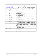
Page 79: ...up time 0 ns tRRE read pulse asserted to ready enabled delay 5 ns 12 ns tRDE read pulse asserted to data enable delay 5 ns 12 ns tRAP ready active pulse width 17 ns 23 ns tRTD ready asserted to data valid delay 5 ns tRCSH read pulse deasserted to chip select deasserted delay 0 ns tRAH address valid to read pulse deasserted hold time 0 ns tRDH data valid enabled to read pulse deasserted hold time 0...

Page 80: ...time 0 ns tWRE write pulse asserted to ready enabled delay 5 ns 12 ns tWDV write pulse asserted to data valid delay 40 ns tRAP ready active pulse width 17 ns 23 ns tWCSH write pulse deasserted to chip select deasserted delay 0 ns tWAH address valid to write pulse deasserted hold time 0 ns tRTW ready asserted to write pulse deasserted delay 0 ns tWDH data valid enabled to read pulse deasserted hold...

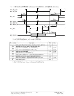
Page 81: ...ime 0 ns tCRE chip select asserted to ready enabled delay 5 ns 12 ns tCDE chip select asserted to data enable delay 5 ns 12 ns tRAP ready active pulse width 17 ns 23 ns tRTD ready asserted to data valid delay 5 ns tCWH write signal inactive to chip select deasserted hold time 0 ns tRAH address valid to chip select deasserted hold time 0 ns tRDH data valid enabled to chip select deasserted hold tim...

Page 82: ... LBU unit drives the ERTEC 200 databus The ERTEC 200 has two LBU chip select inputs One for access to the page configuration register LBU_CS_R_N and one to access to the ERTEC 200 memory address space LBU_CS_M_N Only one of these chip select signals may be active at a time and it is not allowed to change the chip select during the complete access 7 6 Host Interrupt Handling The ERTEC 200 generates...

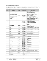
Page 83: ...ex range register 2 Low LBU_P2_RG_H 0x0022 2 bytes W R 0x0020 LBU pagex range register 2 High LBU_P2_OF_L 0x0024 2 bytes W R 0x0000 LBU pagex offset register 2 Low LBU_P2_OF_H 0x0026 2 bytes W R 0x3000 LBU pagex offset register 2 High LBU_P2_CFG 0x0028 2 bytes W R 0x0000 LBU configuration register 2 LBU_P3_RG_L 0x0030 2 bytes W R 0x0800 LBU pagex range register 3 Low LBU_P3_RG_H 0x0032 2 bytes W R...

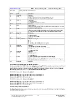
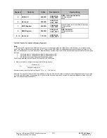
Page 84: ...t setting 15 8 are read write accessible 7 0 are read only value 00h LBU_P0_OF_H W R Addr LBU_CS_R_N 0x06 Default 0x0000_1010 KRAM LBU_P1_OF_H W R Addr LBU_CS_R_N 0x16 Default 0x0000_1000 IRT Reg LBU_P2_OF_H W R Addr LBU_CS_R_N 0x26 Default 0x0000_3000 EMIF LBU_P3_OF_H W R Addr LBU_CS_R_N 0x36 Default 0x0000_4000 Periph Description High word of LBU Pagex_Offset_register Bit No Name Description 15 ...

Page 85: ...aligned can be used Changed Address Mode Hold Address Mode must be set individually for source and target Synchronization signals of UART and SPI for DMA transfers SOURCE DESCRIPTION SPI1_SSPRXDMA RX FIFO not empty SPI1_SSPTXDMA TX FIFO empty UART_UARTRXINTR UART Receive Interrupt UART_UARTTXINTR UART Transmit Interrupt Table 31 I O Synchronization Signals Description of the address modes Change A...

Page 86: ...ption 31 0 START_ADDRESS Start address Only word addresses are permitted bits 0 and 1 are ignored DMAC0DestAddrReg DMA Destination Address W R Addr 0x8000_0004 Default 0x0000_0000 Description Target address oft he data block to be transferred by the DMA controller Bit No Name Description 31 0 DESTINATION_ADD RESS Target address Only word addresses are permitted bits 0 and 1 are ignored DMAC0ContrR...

Page 87: ...een two read access operations Byte count and destination width D_Width must match up If Halfword is selected in D_Width then bit 0 is ignored by byte count considered to be 0 If Word is selected in D_Width then bit 1 0 is ignored by byte count considered to be 00 The DMA is started with Start Abort 1 and stopped during operation with Start Abort 0 The DMA has to be started by setting bit 31 to 1 ...

Page 88: ...ed 4 Auto Negotiation Advertisement Register Extended 5 Auto Negotiation Link Partner Ability Register Extended 6 Auto Negotiation Expansion Register Extended 7 Next Page Timing Register Extended 8 15 Non supported registers 16 Silicon Revision Code Vendor specific 17 ModeControl Status Register Vendor specific 18 Special Modes Vendor specific 19 SMII Configuration Status Register Vendor specific ...

Page 89: ... for at least 100µs In the case of a software reset via the PHY_CONFIG register the reset duration is increased internally to 256µs to stabilize the PLL Each PHY has 6 LED outputs that are routed to the GPIOs 7 0 as an alternative function Four status displays per PHY can be wired to external LEDs The following displays are available in parallel P1 P2_DUPLEX_N Half Full P1 P2_SPEED_N 100BASE TX FX...

Page 90: ...ion Page Received INT2 Parallel Detection Fault INT3 Auto Negotiation LP Acknowledge INT4 Link Down INT5 Remote Fault Detected INT6 Auto Negotiation complete INT7 ENERGY On generated INT8 SMII elastic buffer overflow underflow The external circuitry of the UTP interface and the 100BASE FX is presented in the description xx If the internal PHYs are not used and external PHYs are connected to the MI...

Page 91: ...t ROM Not used all APB interfaces incl Boot ROM all APB interfaces incl Boot ROM 5000 0000 5FFF FFFF 5 ARM ICU Not used Not used Not used 6000 0000 6FFF FFFF 6 Not used Not used Not used Not used 7000 0000 7FFF FFFF 7 EMIF Register Not used EMIF Register Not used 8000 0000 8FFF FFFF 8 DMA Not used Not used Not used 9000 0000 FFFF FFFF 9 15 Not used Not used Not used Not used Table 33 Partitioning ...

Page 92: ...irroring over the entire 16 Mbytes EMIF IO Bank 1 16 MB 3100_0000 31FF_FFFF When a smaller device is interfaced mirroring over the entire 16 Mbytes EMIF IO Bank 2 16 MB 3200_0000 32FF_FFFF When a smaller device is interfaced mirroring over the entire 16 Mbytes EMIF IO Bank 3 16 MB 3300_0000 33FF_FFFF When a smaller device is interfaced mirroring over the entire 16 Mbytes Not used 3400_0000 3FFF_FF...

Page 93: ...re not valid While the 2 Mbyte areas are mirrored within the 8 Mbyte physical address area different access types are used 2 4 Mbyte area for unaligned consistent 16 bit accesses to IRT 4 6 Mbyte area for unaligned consistent 32 bit accesses to IRT 6 8 Mbytes is not supported supplies undefined values The 8 Mbyte address area is mirrored 32 times within the 256 Mbytes 2 Memory areas are mirrored a...

Page 94: ...arators 2 data comparators with filter function 1 trigger input available externally via GPIO 1 trigger output available externally via GPIO 8 memory map decoders for decoding the physical address area of the ERTEC 200 1 1 sequencer 2 counters 1 Supplemental to the ETM0 specification the 8 MMD regions have been decoded via the hardware SEG0 0k 4k Instruction and data access to I cache SEG0 full In...

Page 95: ...an internal pull up resistor at the TRST_N JTAG pin is not included The user has to ensure the proper circuitry for the utilized debugger The standard connector for JTAG interfaces is a 20 pin connector with a pin spacing of 0 1 inch All JTAG pins and the two additional DBGREQ and DBGACK pins are connected here The connector is assigned as follows Function Pin No Pin No Function Vcc Sense 1 2 Vcc ...

Page 96: ...terrupt Request GPIO General Purpose Input Output ICE In Circuit Emulator ICU Interrupt Controller Unit IRQ Interrupt Request IRT Isochronous Real Time ITCM Instruction Tightly Coupled Memory JTAG Joint Test Action Group LBU Local Bus Unit MAC Media Access Controller MII Media Independent Interface MPU Memory Protection Unit PD Pull Down PU Pull Up RT Real Time SPI Standard Serial Peripheral Inter...

Page 97: ...Cell TM Synchronous Serial Port PL021 Technical Reference Manual 7 Embedded Trace Macrocell Architecture Specification ETM_Spec PDF 8 Multi ICE System Design Consideration Applic Note 72 DAI0072A_Multiicedesign Notes PDF 9 IEEE Standard Test Access Port and Boundary Scan Architecture 1149 1 IEEE Boundary Scan 2001 PDF 10 IR35 107 3 pdf 11 LeadfreeIR50_60 pdf 12 Codeexpl pdf 13 PHY_Data_Sheet pdf 1...

Reviews: