background image

Configuration

5-26

7SJ63 Manual

C53000-G1140-C120-1

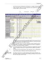
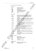
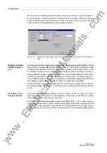
Figure 5-28

Window Information Catalog (Example: Different Command Types) 

If a command with multiple outputs is configured, all binary outputs required in the ma-
trix for the configuration are automatically defined. If one of these outputs is deconfig-
ured, all other binary outputs associated with the command will be automatically de-
configured. 

Please pay attention to the comments and switching examples in Section 5.2.1, par-
ticularly the fixed defined sequence of relay assignments (TRIP before CLOSE). 

When configuring commands, the context menu is dependent on the type of com-
mand. In some cases, the selection latched/unlatched is not available. Instead, the al-
ternatives are 

;

 (configured), 

B

 (not configured), and 

)

 (busy flag). The latter means, 

independent of the switching direction, an indication is always issued during activation 
of the switching device. 

For double commands with a common output, a fourth alternative 

&

 (Common contact) 

appears. Using this, the binary output may be defined as the common relay (common 
contact). When this is the case, several double commands with common contacts may 
be assigned to the same common relay (common contact), thus saving binary outputs. 
This assumes the signals at the common outputs have the same potential. 

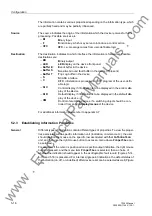
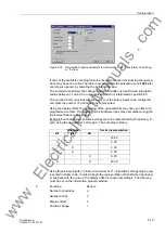
Using the 

2EMHFW3URSHUWLHV

 dialog window, additional properties for commands 

issued to the switching device may be defined. Thus, the operating mode (pulse or 
latched) output of a switching command, the seal-in time for pulse commands, the out-
put delay of the command, and feedback monitoring may be set (see Figure 5-29). The 
output delay is only relevant for equipment which removes an indication before the 
switching is completed. 

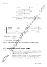
Example: 
Double Command with 
2 Contacts (acc. Table 5-1) 

www 

. ElectricalPartManuals 

. com

Summary of Contents for siprotec 7SJ63

Page 1: ...uction Manual 3UHIDFH 7DEOH RI RQWHQWV QWURGXFWLRQ 1 DUGZDUH DQG RQQHFWLRQV 2 QLWLDO QVSHFWLRQV 3 6 3527 HYLFHV 4 RQILJXUDWLRQ 5 XQFWLRQV 6 2SHUDWRUV 7RROV 7 QVWDOODWLRQ DQG RPPLVVLRQLQJ 8 5RXWLQH KHFNV DQG 0DLQWHQDQFH 9 7HFKQLFDO DWD 10 SSHQGL A QGH w w w E l e c t r i c a l P a r t M a n u a l s c o m ...

Page 2: ...Siemens AktiengesellschaftBuch Nr C53000 G1140 C120 1 w w w E l e c t r i c a l P a r t M a n u a l s c o m ...

Page 3: ...000 compliance for the relays Neither the performance nor the functionality of the protection relays become negatively affected through input of a date which will before during or after the year 2000 The tests were made according the recognized rules of the British Standards Institute BSI Because of the complexity of the application a residual risk regarding the data function may not be totally ex...

Page 4: ... the product or the part of the manual that deserves special attention ANSI This product has been designed according to ANSI C37 90 standards 69CA IND CONT EQ TYPE 1 E194016 IND CONT EQ TYPE 1 Warning During operation of electrical equipment certain parts of these devices are under high voltage Severe personal injury or significant equipment damage could result from im proper behavior Only qualifi...

Page 5: ...PHWHU FRQGLWLRQV or possible settings of parameters that appear in the de vice display or on the screen of a PC with DIGSI 4 are additionally shown in italic style This also applies to selection items for selection menus QQXQFLDWLRQV or identifiers for information produced by the device or required by other devices or from the switch gear is shown in mono script same point size and placed into quo...

Page 6: ...nts Copyright Copyright Siemens AG 1999 All rights reserved Dissemination or reproduction of this document or evaluation and com munication of its contents is not authorized except where expressly per mitted Violations are liable for damages All rights reserved particularly for the purposes of patent application or trademark registration Registered trademarks SIPROTEC SIMATIC SIMATIC NET SINAUT an...

Page 7: ...ruction 2 16 2 2 2 Connections to Threaded Terminals 2 19 2 2 3 Connections to Optical Communication Interfaces 2 19 2 3 Version of 7SJ63 with a Detached Operator Panel 2 21 2 3 1 Construction 2 21 2 3 2 Connections to Threaded Terminals 2 23 2 3 3 Connections to Plug In Terminals 2 27 2 3 4 Connections to Optical Communication Interfaces 2 30 2 3 5 Connections to Electrical Communication Interfac...

Page 8: ...vice Configuration 4 21 4 8 Configuration of Inputs and Outputs Configuration Matrix 4 22 4 9 Display Editor 4 25 4 9 1 Default Display 4 25 4 9 2 Control Display 4 25 4 10 Programmable Logic CFC 4 27 4 11 Power System Data 4 29 4 12 Setting Groups 4 30 4 13 General Device Settings 4 32 4 14 Time Synchronization 4 33 4 15 Serial Interfaces 4 34 4 16 Passwords 4 36 5 Configuration 5 1 5 1 Configura...

Page 9: ...Phase Overcurrent Protection 6 34 6 2 2 4 Programming Settings for Time Overcurrent Ground Protection 6 34 6 2 2 5 Settings for Ground Overcurrent Protection 6 37 6 2 2 6 Information List for Ground Overcurrent Protection 6 38 6 3 Directional Overcurrent Protection 67 67N 6 40 6 3 1 Description of Directional Overcurrent Protection 6 42 6 3 1 1 Definite Time Directional Overcurrent Protection 6 42...

Page 10: ...Element 46 TOC 6 87 6 7 2 Programming Settings 6 89 6 7 2 1 Settings for Negative Sequence Phase Balance Current Protection 6 91 6 7 2 2 Information List for Negative Sequence Current Protection 6 93 6 8 Motor Starting Protection 48 6 94 6 8 1 Description of Motor Starting Protection 6 94 6 8 2 Programming Settings 6 96 6 8 2 1 Settings for Motor Starting Time Monitoring 6 97 6 8 2 2 Information L...

Page 11: ...g 6 142 6 15 Fault Location 6 143 6 15 1 Description of Fault Location 6 143 6 15 2 Setting The Functional Parameters 6 145 6 15 2 1 Settings for Fault Locator 6 146 6 15 2 2 Information List for Fault Location 6 146 6 16 Phase Rotation 6 147 6 16 1 Description of Phase Rotation 6 147 6 16 2 Programming Settings 6 147 6 17 Monitoring Functions 6 148 6 17 1 Description of Measured Values Monitoring...

Page 12: ...ors Tools 7 1 7 1 Retrieval of Information 7 2 7 1 1 Messages 7 2 7 1 1 1 Output of Messages 7 2 7 1 1 2 Event Log Operating messages 7 4 7 1 1 3 Trip Log Fault Messages 7 6 7 1 1 4 GroundFaultMessages GroundFaultmessagesassociatedwiththesensitivegroundfaultfunction 7 8 7 1 1 5 Saving and Erasing the Messages 7 9 7 1 1 6 General Interrogation 7 11 7 1 1 7 Spontaneous Messages 7 11 7 1 2 Statistics...

Page 13: ... Phase Rotation Testing 8 23 8 3 2 Directional Testing With Load Current 8 24 8 3 3 Polarity Testing for Ground Fault Protection 8 25 8 3 4 Testing the Reverse Interlocking Scheme if applicable 8 27 8 3 5 Testing the Breaker Failure Scheme if applicable 8 29 8 3 6 Testing User Defined Functions 8 29 8 3 7 Test Mode and Blocking Data Transmission 8 30 8 3 8 Checking the Binary Inputs and Outputs 8 ...

Page 14: ...and 51N Elements 10 13 10 4 Directional Time Overcurrent Protection 67 and 67N Elements 10 19 10 5 Dynamic Cold Load Pick up Function 50c 50Nc 51Nc 67c 67Nc 10 20 10 6 Inrush Restraint 10 20 10 7 Sensitive Ground Fault Detection 64 50Ns 67Ns 10 21 10 8 Negative Sequence Protection 46 10 23 10 8 1 Definite Time Elements 46 1 and 46 2 10 23 10 8 2 Inverse Time Elements 46 TOC 10 23 10 9 Motor Starti...

Page 15: ...18 A 3 Elementary Diagrams V4 0 A 23 A 3 1 Housing for panel flush mounting or cubicle installation A 23 A 3 2 Housing for panel surface mounting A 28 A 3 3 Devices With Detached Operation Unit A 35 A 4 Connection Examples A 40 A 5 Settings A 48 A 6 Interoperability List A 59 A 7 Information List A 61 A 8 Overview of the masking features of the user defined informations A 96 A 9 Default Settings A...

Page 16: ...xiv 7SJ63 Instruction Manual C53000 G1140 C120 1 w w w E l e c t r i c a l P a r t M a n u a l s c o m ...

Page 17: ...are introduced in this section An overview of the devices is presented in their application characteristics and scope of functions 1 1 Overall Operation 1 2 1 2 Applications 1 5 1 3 Characteristics 1 7 1 4 Scope of Functions 1 8 w w w E l e c t r i c a l P a r t M a n u a l s c o m ...

Page 18: ...r measur ing of the phase currents The use of the fourth input depends on the version of the device ordered The fourth input can be used for measuring the ground current as the residual of the phase current transformers In or for measuring the ground current from a separate current transformer INs 3I0 The latter is used in a highly sensitive ground fault protective scheme INs or as a polarizing 3I...

Page 19: ...cording of messages and data for events alarms faults and control actions and provision of their data for analysis Management of the operating system and the associated functions such as data re cording real time clock communications interfaces etc Binary Inputs and Outputs The µC obtains external information through the binary inputs such as blocking com mands for protective elements or position ...

Page 20: ...physical interfaces are available to suit the particular application Power Supply The 7SJ63 can be supplied with any of the common power supply voltages from 24 VDC to 250 VDC The device can also be supplied with 115 VAC Momentary dips of the supply voltage up to 50 ms are bridged by a capacitor see Technical Data Sub section 10 1 Voltage dips can occur for example if the voltage supply system sub...

Page 21: ... and sensitive ground fault detection for high resis tance ground faults or systems that are resistively grounded 50 Ns 67Ns The highly sensitive ground fault detection can be directional or non directional Other protective functions are available some of which depend on the version of the device that is ordered These additional functions include negative sequence phase balance current protection ...

Page 22: ...uration can be made to the relay Realtime operating quantities can be viewed Waveform capture and Event Log records can be displayed and controls can be issued A DIGSI 4 service interface port a system SCADA port and a time sync port IRIG B or DCF77 are optionally available on the rear of the device A rear service interface can be supplied as RS 232 RS 485 or multimode fiber optics type ST DIGSI 4...

Page 23: ...sary for the proper protection of lines feeders mo tors and busbars Additional protection and control functions available some as options Continuous calculation and display of measured quantities on the front of the de vice Easy devise operation through an integrated operator panel or by means of a con nected personal computer running DIGSI 4 Recording of event data fault data and waveform capture...

Page 24: ...ctional time overcurrent elements are independent of the non directional time overcurrent elements Fault direction is calculated for each phase and direction is determined indepen dently for phase faults using phase phase voltage opposite of the current being compared and for ground faults using zero sequence quantities Dynamic Cold Load Setting Adjustment Dynamic adjustments of the pickup values ...

Page 25: ... current magnitude Additional time constant setting for motors to accommodate both the motor rotating and the motor at standstill Start Inhibit for Motors Rotor temperature is calculated based on the stator currents Start up is permitted only if the rotor has sufficient thermal reserves for a complete start up Disabling of the start inhibit is possible if an emergency start up is required Voltage ...

Page 26: ...ble Processing of measured values including zero suppression adding a knee charac teristic for a transducer input and live zero monitoring Monitoring Functions Availability of the 7SJ63 is greatly increased because of self monitoring of the inter nal measurement circuits power supply hardware and software Current transformer and voltage transformer secondary circuits are monitored us ing summation...

Page 27: ... 1 Tracking of operating hours time when load is supplied of the equipment being protected Commissioning aids such as connection check direction determination and the display of test recordings n w w w E l e c t r i c a l P a r t M a n u a l s c o m ...

Page 28: ...Introduction 1 12 7SJ63 Manual C53000 G1140 C120 1 w w w E l e c t r i c a l P a r t M a n u a l s c o m ...

Page 29: ...ibed Device construc tion is presented The options for terminal connections and communication interfaces are covered Data are given for wire connections and communication connections Information on accessories and tools is given 2 1 Version of 7SJ63 for Panel Flush Mounting Cubicle Mounting 2 2 2 2 Version of 7SJ63 for Panel Surface Mounting 2 16 2 3 Version of 7SJ63 with a Detached Operator Panel...

Page 30: ...e boards are connected to the terminals and sup ported in guide rails of mats that are mounted within the case at the top and bottom Each guide rail has a visible number from 1 to 42 indicating the installation locations of the printed circuit boards The front panel is removable The screws for removing the component are located be hind the four covers at the corners A 7SJ63 with housing size 1 1 h...

Page 31: ...s serve to escape from specific menues or execute changes such as setting changes 5 Numerical Keys These keys serve for entry of numerical values such as protective settings 6 Function Keys Four function keys allow the quick and simple execution of frequently used actions Typical applications include for example jumping to a particular position in the menu tree such as the fault data in the Trip L...

Page 32: ...nts processing or control information and binary in put or output status Next to the LEDs on the front panel a labeling strip is provided on which the user specified LED functions may be written 12 Operating Condition Indicators The two LEDs RUN green and ERROR red indicate the operating condition of the device 13 Coverings for the screws that secure the front panel View of Front Panel Housing Siz...

Page 33: ...ber ports for the service interface at location B Figure 2 3 Rear View of a 7SJ63 Housing Size 1 2 with Screw type Terminals exam ple only 1 2 3 4 5 6 7 8 1 2 3 4 5 6 7 8 9 10 11 12 13 14 15 16 17 18 1 2 3 4 5 6 7 8 9 10 11 12 13 14 15 16 17 18 Ch1 Ch2 A B C F K J UH UH 1 2 3 4 5 6 7 8 9 10 11 12 13 14 15 16 17 18 R Q 1 2 3 4 5 6 7 8 9 10 11 12 P Slave P Master RS232 RS485 w w w E l e c t r i c a ...

Page 34: ...3 Housing Size 1 1 Threaded Contacts are Example Only 1 2 3 4 5 6 7 8 9 10 11 12 13 14 15 16 17 18 Ch1 Ch2 A B C F UH UH P Slave P Master RS232 RS485 1 2 3 4 5 6 7 8 1 2 3 4 5 6 7 8 9 10 11 12 13 14 15 16 17 18 R Q 1 2 3 4 5 6 7 8 9 10 11 12 13 14 15 16 17 18 K J 1 2 3 4 5 6 7 8 9 10 11 12 1 2 3 4 5 6 7 8 9 10 11 12 13 14 15 16 17 18 M L 1 2 3 4 5 6 7 8 9 10 11 12 w w w E l e c t r i c a l P a r t...

Page 35: ...l Blocks for Voltage Connections The two available versions of terminal blocks for voltage connections are shown in Fig ure 2 5 Figure 2 5 Terminal Blocks of Threaded Terminals for Voltage Connections Rear View The numbering system for the threaded terminals is illustrated in Figure 2 6 Figure 2 6 Correlation between Threaded Terminals and Connection Numbers example 18 Terminal 12 Terminal 1 2 3 4...

Page 36: ... hazards to service personnel due to the high voltages that can occur if the sec ondary circuits of the current transformers are open When the I O board is properly inserted into the case of the 7SJ63 the short circuits of the current paths are removed after the transformers of the device are connected to the terminal pairs The short circuit feature of the 7SJ63 is an important and reliable safety...

Page 37: ...r AWG 14 to 10 Use copper wires only Maximum Tightening Torque 2 0 ft lb or 24 in lb 2 7 Nm Short Circuit Links Short circuit links are available for convenience in making terminal connections The links can be used to connect two terminals located on the same side of the termi nal block Thus if the 7SJ63 is the last device in the current transformer circuits the links provide a convenient way to t...

Page 38: ...e removed with a 6x1 mm screwdriver All of the terminal block screws must be tightened to apply a cap There are two types of covering caps as shown in Figure 2 9 Ordering information is provided in Section A 1 in the Appendix Figure 2 9 Covering Caps for Terminal Blocks with Threaded Terminals Covering Cap for 18 Terminal Voltage Covering Cap for 12 Terminal Voltage Connection Terminal Block or 8 ...

Page 39: ...tters Each plug in terminal forms a complete set of connections that consists of three pins arranged as follows Pin a Signal Connection Pin b Common Connection Pin c Shielding Connection The signal pins are the only terminal pins that are directly connected to the internal printed circuit boards of the 7SJ63 Depending on the version of the terminal block 18 or 12 signal connections are provided Re...

Page 40: ...el of the 7SJ63 Depending on the version of the terminal block 18 or 12 shielding connections are provided Figure 2 12 Schematic Diagram of the Plug in Terminal Blocks Connections to Plug In Terminals Connections to plug in terminals are made with pin connectors There are two versions of pin connectors Version 1 2 pin connector Version 2 3 pin connector Signal Connection Common Connection Shieldin...

Page 41: ...eing used Section 0 5 mm2 to 1 0 mm2 e g Bandware 4000 Pieces Type 827039 1 from AMP Corp Individual Piece Type 827396 1 from AMP Corp Section 1 0 mm2 to 2 5 mm2 e g Bandware 4000 Pieces Type 827040 1 from AMP Corp Individual Piece Type 827397 1 from AMP Corp Connection of a conductor to a contact is performed using a hand crimping tool e g type 0 825582 from AMP Co After the wires are crimped the...

Page 42: ...o the left Figure 2 14 Optical Communication Interfaces with Protective Caps Connections to Optical Communication Interfaces Optical Connector Type ST Connector Fiber Type Multimode graded index G optical fiber G50 125 µm G62 5 125 µm G100 140 µm Wavelength λ 820 nm approximately Allowable Bending Radius For indoor cable rmin 2 in 5 cm For outdoor cable rmin 8 in 20 cm Laser class 1 acc EN 60825 1...

Page 43: ...ry communication cables are dependent on the interface EIA 232 Five wire twisted and shielded e g interface cable 7XV5100 4 EIA 485 Three wire twisted and shielded Profibus Two wire or four wire twisted and shielded Wire Type A DIN 19245 Part 2 and EN 50170 vol 2 twisted and shielded Wire Resistance 135 Ω to 165 Ω f 100 kHz Capacitance 30 nF km or 48 nF mile Circuit Resistance 110 Ω km or 177 Ω mi...

Page 44: ...ter and the lower center of the front panel frame must also be removed The front panel has a covered keypad with oper ating and display elements necessary for equipment operation All connections for these elements are combined into an adapter module on the front panel that is linked via a ribbon cable with plug connectors to the internal processor board CPU The nameplate sticker showing important ...

Page 45: ... non inter locked operation 9 Serial Communication Interface 9 pin Female D subminiature connector This serial interface is for the connection of a local PC running DIGSI 4 10 LED Key This key has the dual purpose of resetting latched LEDs and the latched contacts of binary outputs as well as testing all of the LEDs 11 LEDs The function of these indicators can be programmed There is a vast selecti...

Page 46: ... 85 76 52 53 54 55 56 57 58 59 60 62 63 64 65 66 72 67 68 69 70 71 73 74 75 61 36 L L 39 40 41 47 42 43 44 45 46 48 49 50 87 88 89 90 91 97 92 93 94 95 96 98 99 100 85 26 27 28 29 30 31 32 33 34 35 11 12 13 14 15 16 22 17 18 19 20 21 23 24 25 1 2 3 4 5 6 7 8 9 10 124 123 122 121 120 119 118 117 116 125 149 148 147 146 145 144 143 142 141 150 139 138 137 136 135 129 134 133 132 131 130 128 127 126 ...

Page 47: ...2 to 7 mm2 or AWG 20 to 9 Use copper wires only Maximum Tightening Torque 0 9 ft lb 1 2 Nm 2 2 3 Connections to Optical Communication Interfaces Optical Communication Interfaces There are two versions of optical communication interfaces 1 channel and 2 chan nels The optical interface is mounted in a housing that is located on the bottom of the 7SJ63 See Figure 2 18 A front view of the optical inte...

Page 48: ...re replaced with a D subminiature port containing the Profibus interface See Figure 2 19 Figure 2 19 Housing Panel with Optical Communication Interfaces Housing for optical communication interfaces Channel B Channel D Channel C Channel E Channel B Channel D Channel C Channel E Optical communication interfaces Optical communication interfaces and D subminiature connector w w w E l e c t r i c a l P...

Page 49: ...y are in place Each guide rail has a visible number from 1 to 42 indicating the installation locations of the printed circuit boards The printed cir cuit boards are inter connected with ribbon cables and plug connectors The terminals for connecting the 7SJ63 to external equipment are on the rear panel which is bolted to the housing Nameplate stickers which show important information such as the po...

Page 50: ... 14 16 18 a b c 13 11 15 17 9 7 5 3 1 a b c 2 4 6 8 c 10a b 12a 14 16 18 a b c 13 a 11 15 a 17 a b SIEMENS SIPROTEC 1 2 6 3 0 5 4 7 8 9 PICKUP A PICKUP B TRIP PICKUP C PICKUP G ENABLE CB OPEN CB CLOSE TC FAIL 7SJ63 RUN ERROR MENU ESC LED CTRL ENTER F4 F1 F2 F3 Fault Data Meter Breaker Open Remote Normal Local Test Default Display Fault Location With F4 21 kV 1000 A F K J UH CLOSE OPEN Ch1 Ch2 A B ...

Page 51: ...l Blocks for Voltage Connections The two available versions of terminal blocks for voltage connections are shown in Fig ure 2 5 Figure 2 22 Terminal Blocks of Threaded Terminals for Voltage Connections Rear View The numbering system for the threaded terminals is illustrated in Figure 2 6 Figure 2 23 Correlation between Threaded Terminals and Connection Numbers example 18 Terminal 12 Terminal 1 2 3...

Page 52: ...s hazards to service personnel due to the high voltages that can occur if the sec ondary circuits of the current transformers are open When the I O board is properly inserted into the case of the 7SJ63 the short circuits of the current paths are removed after the transformers of the device are connected to the terminal pairs The short circuit feature of the 7SJ63 is an important and reliable safet...

Page 53: ...r AWG 14 to 10 Use copper wires only Maximum Tightening Torque 2 0 ft lb or 24 in lb 2 7 Nm Short Circuit Links Short circuit links are available for convenience in making terminal connections The links can be used to connect two terminals located on the same side of the termi nal block Thus if the 7SJ63 is the last device in the current transformer circuits the links provide a convenient way to t...

Page 54: ... removed with a 6x1 mm screwdriver All of the terminal block screws must be tightened to apply a cap There are two types of covering caps as shown in Figure 2 9 Ordering information is provided in Section A 1 in the Appendix Figure 2 26 Covering Caps for Terminal Blocks with Threaded Terminals Covering Cap for 18 Terminal Voltage Covering Cap for 12 Terminal Voltage Connection Terminal Block or 8 ...

Page 55: ...tters Each plug in terminal forms a complete set of connections that consists of three pins arranged as follows Pin a Signal Connection Pin b Common Connection Pin c Shielding Connection The signal pins are the only terminal pins that are directly connected to the internal printed circuit boards of the 7SJ63 Depending on the version of the terminal block 18 or 12 signal connections are provided Re...

Page 56: ...el of the 7SJ63 Depending on the version of the terminal block 18 or 12 shielding connections are provided Figure 2 29 Schematic Diagram of the Plug in Terminal Blocks Connections to Plug In Terminals Connections to plug in terminals are made with pin connectors There are two versions of pin connectors Version 1 2 pin connector Version 2 3 pin connector Signal Connection Common Connection Shieldin...

Page 57: ...eing used Section 0 5 mm2 to 1 0 mm2 e g Bandware 4000 Pieces Type 827039 1 from AMP Corp Individual Piece Type 827396 1 from AMP Corp Section 1 0 mm2 to 2 5 mm2 e g Bandware 4000 Pieces Type 827040 1 from AMP Corp Individual Piece Type 827397 1 from AMP Corp Connection of a conductor to a contact is performed using a hand crimping tool e g type 0 825582 from AMP Co After the wires are crimped the...

Page 58: ...o the left Figure 2 31 Optical Communication Interfaces with Protective Caps Connections to Optical Communication Interfaces Optical Connector Type ST Connector Fiber Type Multimode graded index G optical fiber G50 125 µm G62 5 125 µm G100 140 µm Wavelength λ 820 nm approximately Allowable Bending Radius For indoor cable rmin 2 in 5 cm For outdoor cable rmin 8 in 20 cm Laser class 1 acc EN 60825 1...

Page 59: ...y communication cables are dependent on the interface EIA 232 Five wire twisted and shielded e g interface cable 7XV5100 4 EIA 485 Three wire twisted and shielded Profibus Two wire or four wire twisted and shielded Wire Type A DIN 19245 Part 2 and EN 50170 vol 2 twisted and shielded Wire Resistance 135 Ω to 165 Ω f 100 kHz Capacitance 30 nF km or 48 nF mile Circuit Resistance 110 Ω km or 177 Ω mil...

Page 60: ...Hardware and Connections 2 32 7SJ63 Manual C53000 G1140 C120 1 w w w E l e c t r i c a l P a r t M a n u a l s c o m ...

Page 61: ...ing the operator control panel on the front of the device and the operator control win dows in DIGSI 4 For personnel inexperienced with the 7SJ63 these checks also provide a quick and simple method for understanding the operation of the control pan el and DIGSI 4 The electrical tests can be done without measuring quantities being applied Observations relevant to long term storage of the device are...

Page 62: ... and hints that are en closed in the packaging The shipping packaging can be reused in the same manner for further shipment Stor age packaging alone for individual devices is not sufficient for shipping If other pack aging is used shock requirements under IEC 60255 21 1 Class 2 and IEC 60255 21 2 Class 1 must be met The device should be in the final operating area for a minimum of two hours before...

Page 63: ...in the operating area for at least two hours This time period allows the device to attain temperature equilibrium and prevents dampness and con densation from occurring Power Up Ensuring safe grounding and applying power supply voltage are sufficient for a first electrical inspection of the device o Connect the ground of the device to the ground of the location The ground of a 7SJ63 designed for f...

Page 64: ...st vanish from the display in which the complete ordering number the version of firmware implemented and the factory number are shown and the default display must appear Depending on the masking of the LEDs some indicators may light up during and after power up w w w E l e c t r i c a l P a r t M a n u a l s c o m ...

Page 65: ...ete ordering number of the device the version of firmware imple mented and the serial number q When the device is ready for operation first press the key The 0 1 0 18 ap pears q Using the key select the menu item 6HWWLQJV and move to the device set tings using the key The 6 77 1 6 menu appears as shown in Figure 3 1 q Using the key select the menu item 6HWXS WUDV and switch to the selection 6 783 ...

Page 66: ...nd move to the 9 17 2 menu using the key The last quantity in the upper right corner of the display indicates the number of event messages stored in memory The number before the slash indicates the message presently being displayed Upon entering the menu the latest newest message is shown The date and time of the event are shown in the display line above the mes sage q Use the key to read other ev...

Page 67: ...lection 6 783 75 6 using the key See Figure 3 3 q Using the key select the menu item RQWUDVW q If a change of the contrast of the integrated LCD is desired press the key The existing setting appears in a frame with a blinking cursor q Overwrite the present setting with the desired setting using the numerical keys The setting range is 11 to 22 q Confirm the change with the key or cancel the change ...

Page 68: ... examples as descibed below To perform the steps in the examples first connect the SIPROTEC 4 device to the PC and match the DIGSI 4 interface data with the equipment To accomplish this task q Establish a physical connection between a serial interface of the PC and the oper ating serial interface of the device on the front panel q Open the DIGSI 4 application in the PC q Generate a new project by ...

Page 69: ...communication transfer format transfer speed through the interface Figure 3 6 Plug Play Dialog Box for Communication between Device and PC A direct connection is then established on line the data are exchanged between the PC and the device and the initial window for DIGSI 4 opens as shown on Figure 3 7 q By double clicking 2QOLQH in the navigation window left window the structure opens directory t...

Page 70: ... present date and time are shown in the data window right as illustrated in Fig ure 3 8 q Double click on this entry in the data window Figure 3 8 DIGSI 4 Viewing the Secondary Operating Measured Values A table of the secondary operating measured values appears as shown in Figure 3 9 Since no AC currents or voltages are present all measured values are close to zero Deviations of the last digit are...

Page 71: ...ation for an event is provided with a description of the event The corre sponding cause value ON or OFF and date and time of the event are given The events are listed chronologically the newest message is shown first Figure 3 10 DIGSI 4 Event Log Messages Window Example q Press the key on the device all LEDs should light while the key is pressed q The message Reset LED appears as the newest messag...

Page 72: ...d the approximate present time according to the device The day of the week is automatically derived from the date and cannot be edited Edit the input fields DWH and 7LPH The format depends on your regional settings of the PC See Figure 3 12 Date mm dd yyyy or dd mm yyyyy Time hh mm ss Click 2 to download the entered values to the device The former values are changed and the dialog field is closed ...

Page 73: ...ot lead to condensation or ice buildup After extended storage the power supply of the device should be energized for one or two days to regenerate the electrolytic capacitors in the power supply This procedure should also be done prior to the device being put in service Under extreme climatic conditions tropics preheating is achieved at the same time and condensation is pre vented After long stora...

Page 74: ...Initial Inspections 3 14 7SJ63 Manual C53000 G1140 C120 1 w w w E l e c t r i c a l P a r t M a n u a l s c o m ...

Page 75: ... the functions discussed may not be available Details about the extent of the functions of the devices the individual settings and the representation structure of the system data are found in the following sections and the DIGSI 4 instruction book 4 1 General 4 2 4 2 Operator Control Facilities 4 5 4 3 Information Retrieval 4 9 4 4 Control 4 15 4 5 Manual Overwrite Tagging 4 17 4 6 General Setting...

Page 76: ...urity in establishing the devic es correct responses Device errors are recognized and quickly annunciated by inte grated self monitoring routines Failure of protection during a fault is therefore almost entirely prevented The user can choose devices with separate protective and process control functions or select a solution that implements both requirements The following solutions are available q ...

Page 77: ...ion of Field Devices in the SICAM Station Control System example Refer to the sample configuration in Figure 4 1 In the case when data is transmitted from the field devices it can be processed in the sub station control device SICAM SC displayed at the operating and observation station SICAM WinCC and transferred by the remote terminal unit interfaces via the network channels to SCADA In the case ...

Page 78: ...ons are breaker control retrieval of information or changing of setting groups All of the operations can also be performed using the HMI on the front of the SIPROTEC 4 device 4 1 5 Waveform Capture DIGSI 4 can also be used to retrieve waveform data and SER information captured by the SIPROTEC 4 device The DIGRA 4 software program can then be used to provide several different graphical representati...

Page 79: ...The features of the displays in the HMI can be q Default Display with pure display features e g switchgear status messages mea sured values etc q Control display configured to appear similar to the default display but including dy namic symbols Control for primary equipment can be performed from this control display Figure 4 2 SIPROTEC 4 Device HMI with Full Graphical Display example SIEMENS SIPRO...

Page 80: ... the to keys the key for a decimal point and the key for a negative sign If a value of infinity is desired press the decimal point key twice appears in the display q The to keys are programmable The keys are typically used to execute com monly performed actions Labeling strips are provided q Latched LEDs and binary outputs are reset and the group of LEDs are tested with the key dual purpose LEDs q...

Page 81: ...140 C120 1 q Two key switches are provided for fast and reliable access to Switching between local and remote control and Switching between interlocked NORMAL and non interlocked TEST operation w w w E l e c t r i c a l P a r t M a n u a l s c o m ...

Page 82: ...this matrix The setting options are presented in an easy to read tabular format Parts of the matrix can be minimized or expanded as desired to simplify the displayed sections and therefore the setting process Filter functions can reduce the size of the matrix to display only relevant information Passwords Password entry is required for tasks such as changing settings executing control commands or ...

Page 83: ... system then information transfer can take place via a connection to the system interface of the SIPROTEC 4 device to q SCADA or q substation controller device e g SICAM SC Local On site the HMI of the SIPROTEC 4 device can be used to retrieve information DIGSI 4 Information retrieval is simple and fast when DIGSI 4 is used For local use connect a PC to the operating serial interface at the front ...

Page 84: ...for devices with sensitive ground fault detection q General Interrogation Display of present condition messages q Spontaneous Annunciation Continuous display of important messages from the device e g after faults control operations etc This feature is very helpful during commissioning k451 gif Figure 4 3 DIGSI 4 Annunciation Display in DIGSI 4 To view the indications in the DIGSI 4 Tool 2QOLQH Sel...

Page 85: ...erating Messages in the Event Log Exam ple Figure 4 5 SIPROTEC 4 Device Display Trip Log and Ground Fault Messages Example 1181 7 21 YHQW RJ 7ULS RJ 0 1 0 18 QQXQFLDWLRQ 0HDVXUHPHQW 9 17 2 5HVHW 21 75 3 2 DVW DXOW QG DVW DXOW 67 8 7 1HWZRUN DXOW 21 5281 8 7 DVW DXOW QG DVW DXOW 67 8 7 URXQG DXOW 21 w w w E l e c t r i c a l P a r t M a n u a l s c o m ...

Page 86: ...values relative to nominal ratings q Other values including thermal values and user defined values q Statistics values k452 gif Figure 4 6 DIGSI 4 Measured value display Example Display in DIGSI 4 To display the measured values using the DIGSI 4 2QOLQH control panel Select 0HDVXUHPHQW in the navigation window The measured value groups ap pear in the data window Double click on a group for example ...

Page 87: ... 17 2SHUDWLRQ SUL 2SHUDWLRQ VHF 0 1 0 18 QQXQFLDWLRQ 0HDVXUHPHQW 0 685 0 17 2SHUDWLRQ SUL 2SHUDWLRQ VHF 23 5 7 21 35 D E Note Measured values can also be displayed in the default display and the control display Prior to this the measured values to be indicated have to be configured in Masking I O Configuration Matrix under settings in DIGSI 4 Then their position within the LCD displays can be desi...

Page 88: ...ert the oscillographic data into graphical rep resentations that can be used to analyze the fault or the event captured by the device DIGRA 4 calculates additional values from the waveform data e g impedances and rms values and displays the captured and calculated values in q Analogue Curves with timebase Time Signals q Vector Diagrams q Circle Diagrams and q Harmonic graphs digra009 Figure 4 8 DI...

Page 89: ...device on site or communicate with the SIPROTEC de vice using a modem and the service interface DIGSI 4 must operate in the On line mode for this function Select RQWURO in the Navigation window and double click on UHDNHU 6ZLWFKHV in the data window In the dialog window that follows all relevant primary control equipment is displayed in a table with the present status Enter the intended device posi...

Page 90: ...lly using the CFC logic too Standard interlockings such as ground switch closed status indication are already contained in the basic settings of the device when delivered from the factory Command Process ing Times Details about the command output time checkback indication monitoring time etc are entered within the framework of the settings Event Recording All control operations are recorded in the...

Page 91: ...ng the wires This function is activated using the HMI 0DLQ 0HQX RQWURO UHDNHU 6ZLWFK 6HW 6WDWXV Tagging To identify unusual operating conditions in the power system tagging can be done The tagging can for example be entered as additional operating conditions in inter locking checks which are set up with CFC Tagging is configured in the same way as for operating devices The status of the tagging is...

Page 92: ...special logic functions CFC q Design of the control display q Specific Settings q Settings for all elements to be used q Settings of the protective functions q Settings of the process control functions Settings are first done Off line The settings are then loaded into the SIPROTEC 4 device on site using the operating serial interface or remotely by modem and the ser vice interface K450 gif Figure ...

Page 93: ...rds Setting steps partially build on the decisions from the previous steps By following the sequence listed unnecessary changes and rework are avoided The sequence en sures that information required for an individual step will be available To design the control display for example the physical connections between the de vice and the primary equipment must be known These connections are determined ...

Page 94: ...e settings on the LCD using 0DLQ 0HQX 6HWWLQJV e g 0DVNLQJ 2 Change settings such as date and time using 0DLQ 0HQX 6HWWLQJV 6HWXS WUDV Figure 4 12 Changing Settings using the HMI Example 0 1 0 18 QQXQFLDWLRQ 0HDVXUHPHQW RQWURO 6HWWLQJV 7HVW LDJQRVH 6 77 1 6 HYLFH RQILJ 0DVNLQJ 2 3 6 VWHP DWD URXS URXS URXS URXS KDQJH URXS 2VF DXOW 5HF 6HWXS WUDV HYLFH FWLYH URXS LV Note Online changes to the indiv...

Page 95: ...ration area of the settings To specify the active functions using DIGSI 4 Double click on HYLFH RQILJXUDWLRQ in the data window Click on the individual fields and select the functions to be enabled e g 66 Startup Counter for Motors k453 gif Figure 4 13 DIGSI 4 Setting the Device Configuration Example The Device Configuration can be viewed from the HMI on the SIPROTEC 4 device In the main menu sele...

Page 96: ...ing indications q Function key F freely programmable key on the HMI e g assigned to trigger events q CFC Programmable logic user specific logic outputs as the origin of the informa tion q Destination of the information with q Binary outputs for the output of signals q LED display of information e g messages q System interface transmission of information e g to SCADA or substation control ler q CFC...

Page 97: ...iew so that the user can combine only the sections of the total matrix that are relevant New Information A further function of the configuration matrix is the capability to define new information This is accomplished by inserting a new line assigning the appropriate information type and configuring the source with an output binary outputs LED etc The new information can also be displayed in the LC...

Page 98: ... is derived from the 6RXUFH column Displays If information is to be displayed in the default display or the control display then enter the settings in the Destination Display columns Information for symbols for a switch gear device that is to be controlled from the control display e g circuit breaker must always be assigned in the Control Display column Details can be found in the DIGSI 4 instruct...

Page 99: ...rix for the default display can be shown The Display Editor program is used to modify the diagram in the display See Figure 4 17 4 9 2 Control Display SIPROTEC 4 devices with graphical displays are delivered with a control display that has default settings and a default layout Individual designs for the control display can be done Catalogs of symbols primary equipment representations and lines are...

Page 100: ...sign of a control display are found in the Display Editor instuction book Order Number E50417 H1176 C095 Abzweig gif Figure 4 17 DIGSI 4 Display Editor Default Display Example Control Display is Similar Note The control display and the default display are generally constructed in the same man ner The same aids are used to design both displays w w w E l e c t r i c a l P a r t M a n u a l s c o m ...

Page 101: ...r the requirements of process control engineering e g MAX MIN etc are available The CFC modules are combined to form complete CFC Logic Functions in order to q perform system specific checks interlocking q generate messages if measured values approach a critical value or q build group messages for transfer to higher level control systems k4122 gif Figure 4 18 DIGSI 4 CFC Basic Options Example CFC ...

Page 102: ...SIPROTEC 4 Devices 4 28 7SJ63 Manual C53000 G1140 C120 1 Figure 4 19 CFC Logic example w w w E l e c t r i c a l P a r t M a n u a l s c o m ...

Page 103: ...cuit breaker or primary switchgear information including a current threshold set ting that is used to indicate the open close position of the primary equipment in sev eral protection functions k4124 gif Figure 4 20 DIGSI 4 Window for Setting the Power System Data 1 example Power System Data 2 Power System Data 2 are part of the setting groups which can be switched over dur ing operation see chapte...

Page 104: ...or the existing configuration of the net work being protected In other words the protection and control can be changed as the network changes The setting groups are saved in the device The setting groups can be changed during operation using DIGSI 4 from the HMI on the device by triggering binary inputs or via the system interface k4114 gif Figure 4 21 DIGSI 4 Entering Settings in Setting Group A ...

Page 105: ...he function f Figure 4 22 DIGSI 4 Entering Settings for a Protective Function example Changing Setting Groups The setting groups can be changed during operation using DIGSI 4 from the HMI on the device by triggering binary inputs or via the system interface The active setting group is indicated Figure 4 23 SIPROTEC 4 Device Changing Setting Groups on the HMI URXS URXS URXS URXS LQDU QSXW via proto...

Page 106: ...faults on the LEDs and the LCD on the front of the SIPROTEC 4 device are defined in the DIGSI 4 window shown below k4123 gif Figure 4 24 DIGSI 4 General Device Settings Targets example The setting can also be changed at any time using the HMI on the SIPROTEC 4 de vice 0DLQ 0HQX 6HWWLQJV HYLFH w w w E l e c t r i c a l P a r t M a n u a l s c o m ...

Page 107: ...ected via a 9 pin D subminiature port on the back panel of the device Setting of the time synchronization is done exclusively with DIGSI 4 Double click on 7LPH 6 QFKURQL DWLRQ in the data window and enter the set tings ka455 gif Figure 4 25 DIGSI 4 Setting of the Time Synchronization example Readout in the HMI Using the SIPROTEC 4 device HMI the time synchronization settings can be checked 0DLQ 0H...

Page 108: ...iagnostic facilities e g DIGSI 4 via modem and or a star connection All DIGSI 4 operations are possible via this interface q The PC interface at front is used for on site connection of a PC on which DIGSI 4 is installed All operations that are possible using DIGSI 4 can be done at this in terface In the DIGSI 4 Interface Settings window under Serial Ports there are among other items settings for q...

Page 109: ...ettings can be checked using the SIPROTEC 4 device HMI In the main menu select 6HWWLQJV 6HWXS WUDV 6HULDO 3RUWV follow ing menus Figure 4 28 Readout of Serial Interface Settings from the HMI example 6 5 32576 URQW 3RUW 6 VWHP 3RUW 6HUYLFH 3RUW 6 783 75 6 DWH 7LPH ORFN 6HWXS 6HULDO 3RUWV HYLFH 0 9HUVLRQ RQWUDVW Note The interface for connecting a time control device is described in the Sub section ...

Page 110: ...ettings q Hardware test menus q Setting Groups ka458 gif Figure 4 29 DIGSI 4 Window Indicating the Active Passwords example When using DIGSI 4 or the HMI on the SIPROTEC 4 device a password is request ed for the specific function Note Password protection against unauthorized access is only in place during on line op eration The passwords for setting changes are first activated when the settings ar...

Page 111: ...e new password again and 2 k4119 gif Figure 4 30 DIGSI 4 Changing Passwords Passwords are numbers up to 8 digits At delivery all passwords are set to 000000 n Note If the password for setting group switching has been forgotten a temporary password can be received from Siemens The temporary password can be used to define a new password for this function The registration number of the DIGSI 4 softwa...

Page 112: ...SIPROTEC 4 Devices 4 38 7SJ63 Manual C53000 G1140 C120 1 w w w E l e c t r i c a l P a r t M a n u a l s c o m ...

Page 113: ...finable functions need to be performed in CFC Continuous Function Chart What should the displays look like Which interfaces are to be used Which time source is to be used to synchronize the internal clock This chapter describes in details how to configure the 7SJ63 5 1 Configuration of Functions 5 2 5 2 Configuration of Information Meaured Values and Commands 5 6 5 3 Creating User Defined Function...

Page 114: ...re not displayed dur ing detailed settings Determination of Functional Scope Configuration settings must be entered using a PC and the software program DIGSI 4 and tranferred via the front serial port or via the rear DIGSI 4 serial port interface Operation via DIGSI 4 is described in Chapter 4 as well as in the DIGSI 4 manual order number E50417 H1176 C097 Entry of password No 7 for setting modifi...

Page 115: ...LWH 7LPH RQO should be selected Additionally depending on the relay model ordered various inverse time characteristics are available based on either IEC standards or ANSI standards or user defined characteristics may be specified A user defined characteristic can include both a tripping and a reset characteristic Non directional overcurrent protection may be defeated during configuration by select...

Page 116: ...rac teristics available for 67 TOC Selection of 67 TOC automati cally enables 67 116 67N 67N TOC Disabled Definite Time only Time Overcurrent Curve IEC Time Overcurrent Curve ANSI User Defined Pickup Curve User def Rese Definite Time only Determines if directional ground definite time 67N and inverse time 67N TOC elements are enabled and the general charac teristics available for 67N TOC Selection...

Page 117: ...sabled Automatic reclosing 180 Fault Locator Disabled Enabled Disabled Fault locator 182 74 Trip Ct Supv Disabled with 2 Binary Inputs with 1 Binary Input Disabled Trip circuit e g breaker monitor ing and method using one binary input or two Adr Setting Setting Options Default Setting Explanation w w w E l e c t r i c a l P a r t M a n u a l s c o m ...

Page 118: ...tion 5 2 1 Preparation Before configuration is started the overall interfacing requirements must be assessed The required inputs and outputs must be compared with the number of physical inputs and outputs present on the relay The types of indications and commands and their requirements should be taken into account Indications Some indications may be device information regarding events and conditio...

Page 119: ...uts contacts For this the corresponding output con tacts are numbered consecutively This must be observed when wiring the relays to the corresponding equipment to be controlled Table 5 1 shows the most important command types They are made available as op tions in the Configuration Matrix for the SIPROTEC device see also Binary Outputs for Switching Devices in Sub section 5 2 4 All double commands...

Page 120: ... CC Relay Contact is Common CCC Relay Contact is Common to a Bus V V Control Voltage Figure 5 4 Single Command with Single Output Double Command with Double Outputs With 4 contacts without feedback with feedback B B Double Command with Double Close and Single Trip Outputs With 3 contacts without feedback with feedback B B Double Command Motor Control left right direction With 2 relays 2 contacts e...

Page 121: ...C t C C V V Relay Configuration Command CLOSE Command TRIP C X BO 1 C X 2 CLOSE TRIP Switching Device COIL COIL CLOSE Command C C TRIP Command CC t C C V V CC Relay Configuration C X BO 1 C X 2 3 X CC CLOSE TRIP Switching Device COIL COIL CLOSING Command C C TRIPPING Command CCC t Switching Device 2 n C C V V CCC Relay Configuration C X BO 1 C X 2 X CCC n CLOSE TRIP Switching Device COIL COIL w w ...

Page 122: ...igure 5 9 Double Command with Double and Single Contacts with 3 Ralays Note It is recommended to mask Trip and Close commands from a protection function the same binary I O s if they operate the same breaker If for instance the Close com mand of the Control function uses two contacts the auto reclose function should be masked also to both contacts See elementary diagrams in the appendix A CLOSING ...

Page 123: ...ct that the same output relays are controlled by two separate commands the grounding command and the isolating command When a trip is initiated the motor rotates in one direction to close the ground switch and in the opposite direction to open the isolating switch Therefore one of the two commands must be negated For this reason command types 5B and 5B 1 are applicable in this situation CLOSING Co...

Page 124: ...ps are described in Section 5 2 3 and configuration is demonstrated in Section 5 2 4 Configuration of information is performed using a PC and the DIGSI 4 software pro gram via the operator or service interface The configuration is represented in DIGSI 4 as a matrix Figure 5 13 Each row is assigned to relay information It is identified by a function number brief text display text an explanation lon...

Page 125: ... is shown but also the type of configuration For example information regarding an event which is configured for display on a LED may be latched or unlatched The possible combinations of information and interfaces is dependent on the informa tion type Impossible combinations are mostly filtered out by DIGSI 4 plausibility checks The matrix columns are divided into three types Information Source and...

Page 126: ...ary outputs etc the abbreviations of all destinations are shown separated by commas If there is not enough room in the cell for the simultaneous display of all abbreviations a double click on the cell and movement of the text cursor within the cell will show the entire contents of the cell To switch between standard view and short view the menu item 9LHZ can also be used The width of the matrix ca...

Page 127: ...uble Command with Single Trip Outputs and Double Close Outputs without feedback CF_D12 Double Command with Single Trip Outputs and Double Close Outputs with feedback C_D3 Double Command 3 relays with Single Outputs and Common Output without feedback CF_D3 Double Command 3 relays with Single Outputs and Common Output with feedback C_D4 Double Command 4 relays with Double Outputs without feedback CF...

Page 128: ...ication the right mouse button is pressed and the menu item 3URSHUWLHV is selected then a choice of whether the indication should appear in the oscillographic fault record Figures 5 14 5 15 and 5 16 is presented For internal single point indications the default status of the indication on off or undefined after device reset can be selected as well Figure 5 15 BI Binary input F Function key which m...

Page 129: ...gle Point Indication IntSP Singe Point Indica tion SP Figure 5 16 Information Properties Example for Information Type Single Point Indication SP Double Point Indi cation DP In addition to the properties entered for single point indications a Suppress interme diate position check box is available which may be checked to suppress the interme diate indication during operations If this field is marked...

Page 130: ...ed when the new state continues to exist after a preset time interval in milliseconds The setting range is from 0 to 86 400 000 ms or 24 hours Whether or not the filter interval is restarted for each change of state during the filtering filter re triggering is selectable It is also possible to set chatter suppression for each indication Figure 5 16 The con tact chatter settings themselves are set ...

Page 131: ...ed Using the display offset the beginning of the evaluated bits may have an offset of a programmed number The stepping of the transfomer taps may be modified using the tap interval feature see example Example Four transformer position settings are to be represented by three binary in puts using the designators 3 through 6 The encoding is binary Using three binary inputs 3 bits a maximum of 23 8 po...

Page 132: ...ertain amp val ue the following values are entered in window according to Figure 5 19 The Dimension is A amps The Conversion Factor is 150 150 A corresponds to 100 input current The limit value upon startup is set for 120 A Metered Values For metered values the determination of the polarity is determined by the direc tion of power flow Figures 5 20 and 5 21 The user may also define the transfer of...

Page 133: ... and entered by the user Such user defined groups and information may be deleted at any time in contrast to predefined groups and information In order to insert a new information group click on a cell within a group that is next to the location where the new group should be located After pressing the right mouse button a context menu should appear Figure 5 22 Figure 5 22 Dialog Box to Insert a New...

Page 134: ...e information groups Annuncia tions Commands Measured Values and Counter Values To insert a specific information unit into an information group it should first be selected in the catalog and using the left mouse button it should then be dragged from the in formation catalog window to a group area on the left of the matrix After the mouse button is released the new information unit is inserted into...

Page 135: ...t mouse button and use the displayed pull down menu to make the entry In certain cases the pull down menu will offer configured or B not configured as the configuration choices In other cases more alternatives will be offered e g latched 8 unlatched and B not configured Entries resulting in an implausible configuration are blocked and inaccessible to the user Configuring Binary Inputs as Sources S...

Page 136: ...urces in order to establish a link using CFC In this situation each function key may be linked with only one internal indication A function key may be occupied because it has al ready been set as an operating function for the relay As delivered from the factory the device s function keys F1 F2 and F3 are preconfigured In order to configure a new indication select one of the options OPEN CLOSE ON O...

Page 137: ...ch output relay be sides of the logic function itself whether it should be latched or unlatched 8 If latched is selected the output relay remains engaged even after the indication is no longer present It must be manually reset by pressing the LED Reset button on the front panel of the relay or via a binary input with the indication function 5HVHW or via the serial SCADA interface If unlatched is s...

Page 138: ...tching direction an indication is always issued during activation of the switching device For double commands with a common output a fourth alternative Common contact appears Using this the binary output may be defined as the common relay common contact When this is the case several double commands with common contacts may be assigned to the same common relay common contact thus saving binary outp...

Page 139: ... of the protective functions or elements in the relay has picked up OPEN commands in contrast can always be executed Please be aware activa tion of thermal overload protection or sensitive ground fault detection can create and maintain a fault condition indication and can therefore lead to the blocking of CLOSE commands If the blocking by protection facility is disabled consider that a blocked res...

Page 140: ...n the buffer with the time of its arrival RR on off the indication is stored in the buffer with the time of its arrival and de parture B not configured the indication is not stored in a buffer Configuring the SCADA Interface as a Destination Depending on the SCADA interfaces connected to the relay the types of information displayed in Table 5 3 may be configured By placing an in the matrix cell th...

Page 141: ... values then become available in the device display in the assigned measurement window Configuring the Metered Value Window as a Destination In addition to the metered values available in the device user defined pulse and me tered values derived from the measured values may be configured into the metered value window so that they may be shown at the front display Retrieving Device Configurations f...

Page 142: ...2 is also given as 0 not active If binary input is active a 1 is displayed Assignment of LEDs may be indicated at the relay itself using a replaceable labeling strip with plain text on the front panel located directly next to the LEDs Preset Configura tions The pre set configurations of the binary inputs and outputs are shown in the overview circuit figures Appendix A 2 The preset configurations f...

Page 143: ...ADA has taken place Figure 5 32 Dialog Box to Restore Metered Values and Program Cyclical Restoration In the current version of DIGSI 4 triggering occurs based on the programmed Absolute time LED 4 Pickup Phase C Non Directional Phase C Directional Phase C Pickup by Cφ Element LED 5 Pickup G Non Directional G Directional G Pickup by Ground Element LED 6 Measurement Failure Fault ΣI Fault I Symmetr...

Page 144: ...ked The time interval begins with the first activa tion of a signal to the binary input 1XPEHU 2I KDWWHU 7HVWV This number represents how many check cycles should be conducted before the binary input is finally blocked Please consider that even a high set value can be reached over the normal life span of the device and could lead to blocking of the binary input Therefore this value can also be set...

Page 145: ...l so the indication RQWDFW FKDWWHU ILOWHU reports this condition Both mes sages are shown in the operating buffer Chattering of a single point indication is set as ON asserted if the binary input has been in an active state Chattering of a single point indication is set as OFF deasserted if the binary input has been in an inactive state If this behavior causes undesired results in individual situa...

Page 146: ...ill appear The desired CFC chart for processing can be selected via a double click of the mouse The CFC program will begin and the chart will be displayed If no chart is available yet you can create a new chart via the menu UHDWH KDUW Run Time Proper ties The functions to be implemented in CFC may be divided into four task levels Measured Values This task is processed cyclically every 600 millisec...

Page 147: ...terlocking condition at the moment of a control operation may not be processed at the right time since meter processing is done only every 600 ms Table 5 5 Selection Guide for Function Modules and Task Levels Function Modules Description Task Level MW_BEARB Meter processing PLC1_BEARB Slow PLC PLC_BEARB Fast PLC SFS_BEARB Interlocking ABSVALUE Magnitude calculation X AND AND Gate X X X BOOL_TO_CO ...

Page 148: ...rd Please refer to the CFC manual The necessary function modules FM are contained in a library located to the right of the configuration chart The module also indicates to which of the four task levels MW_BEARB PLC1_BEARB PLC_BEARB SFS_BEARB it is assigned The modules possess at least one input and one output In addition to these inputs and outputs which are displayed on the configuration sheet a ...

Page 149: ... appear By selecting one of these signals and activating with 2 the selected signal is entered into the left border panel and from there a connection is created to the module input Selection of an output is done in the same manner A connection between two modules is established by a simple se quential clicking on the two connections If the link line display becomes unwieldy or impossible because o...

Page 150: ...exceeded because adverse effects to the protective functionality e g slower trip times would result Table 5 7 Maximum Number of Modules per Process Area for SIPROTEC 7SJ63 The limits are monitored by the DIGSI 4 operating program When 100 of the al lowed memory is used DIGSI 4 issues a warning message See Figure 5 40 Table 5 6 Maximum Number of Charts and Inputs Limit Description Limit Comment Tot...

Page 151: ...own in Appendix A 6 Example 1 MW Under Current Set Points ANSI 37 A configuration for low current monitoring alarm see Figure 5 42 which can be pro duced using CFC should be a first example This element may be used to detect op eration without load or to recognize open circuited conditions By connecting mea sured current values with a limit function via an OR function an indication may be generate...

Page 152: ...SE and TRIP indications from the auxiliary contacts of each switch are used Function modules NOR 2 required XOR and AND are taken from the library and copied into the working page The inputs of the AND gate are increased to 7 The CLOSE indications from the circuit breaker CB and from the grounding switch GS are supplied to the inputs of the NOR functions The OPEN indications from the circuit break...

Page 153: ...utput information indication from the circuit breaker interlocking logic CB TRIP and a joint indication from all protective element trip signals Protection TRIP are linked to a new LUFXLW UHDNHU 7ULS message Furthermore the single point indication SP 7HVW 2SHU which may be coupled via a binary input is coupled with an internal reusable 7HVW RSHU mes sage Figure 5 44 Additional Logic as an Example ...

Page 154: ...in the configuration matrix A library is provided which contains symbols for circuit breakers isolation switches and grounding switches and other devices The standard setup may be modified at any time using the DIGSI 4 diagram editor User defined symbols may also be cre ated and saved in the library The user may assign various symbols to any operating equipment condition in the di alog window pres...

Page 155: ...ed in a LQN dialog window see Figure 5 46 from which the user may click on the desired option and confirm with 2 In this manner the user may link the graphical diagram with configuration settings Position text as necessary by clicking on 7RROV and then QVHUW 7H W and then on the text insertion location in the diagram Figure 5 46 DIGSI 4 Selection Window for Switching Equipment example w w w E l e ...

Page 156: ... clicking 9LHZ 1RUPDO VL H see Figure 5 47 Save the default display and end the Display Editor session by clicking LVSOD ORVH Answer the confirmation with HV Figure 5 47 Default Display in Normal Size View In order to use the default display for further applications e g as a template in other bays or for a control diagram click on LVSOD 7HPSODWH 6DYH DV Se lect the desired save path and enter the ...

Page 157: ...SI 4 The basic procedure is the same as for creating the default display see Section A precondition for modification or creation of dynamic symbols in a control diagram is the configuration of the switching devices used in the control diagram and their re spective feedback indications as described in Section 5 2 This is the only way the di agram may correspond dynamically to present equipment cond...

Page 158: ...see Figure 5 49 In the 3URSHUWLHV HYLFH dialog window which appears the user should select the option 2EMHFW RSHUDWRU FRQWUROODEOH The user should determine which equipment is selected first as a default in the con trol diagram For this select the equipment and then select the option HIDXOW REMHFW The selection should be confirmed by clicking 2 Figure 5 49 Making Equipment Operable and Selecting t...

Page 159: ...ction de vice with setting options for the interfaces Figure 5 50 DIGSI 4 Settings of the PC Interface Serial Port on PC In the first tab the user should enter the communication port of the PC 20 20 etc which is connected to the 7SJ63 relay Manual entry of settings for data format and baud rate can not be entered since these values were taken from the 3 SRUW RQ GHYLFH tab or the 6HUYLFH SRUW tab i...

Page 160: ...on and baud rate differences For good data transmission between modems a setting of sec is recommended For poor connections this value should be increased Large values slow down communications in case of errors When using a direct PC connection 0D PHVVDJH JDSV may be set to sec Other Interfaces Enter specific settings and addresses to identify devices in the other tabs or check the preset values D...

Page 161: ...e using the operator interface at the device itself The user may access the setting page for the interface via 0 1 0 18 through 6HWWLQJV 6HWXS WUDV 6HULDO 3RUWV Under the menu title 6 5 32576 the user will find Front Port System Port and Service Port and selections may be made using the navigation button By pressing the button the sub menu for a particular interface can be accessed The display and...

Page 162: ...03 PROFIBUS External minute impulses via binary input Time Synchroniza tion Settings for time synchronization may be found in DIGSI 4 under 6HWWLQJV 7LPH V QFKURQL DWLRQ Figure 5 54 Figure 5 54 Setting Window inDIGSI 4 To open the 7LPH 6 QFKURQL DWLRQ RUPDW window the user should double click on 7LPH 6 QFKURQL DWLRQ See Figure 5 55 Note The device is delivered from the factory with the internal RT...

Page 163: ...rce fails the internal clock continues unsynchronized If time synchronization is to take place via a control system the option or 352 86 06 must be selected Figure 5 55 When using radio clock signals the user must take into account that it can take up to three minutes after device startup or restored reception for the received time signal to be decoded The internal clock is not resynchronized unti...

Page 164: ...ion even longer Changing the Syn chronization Mode When changing synchronization mode the hardware will re synchronize to the new source within one second This causes breakdown of cyclical synchronization and the internal clock will be disrupted as at startup until the new synchronization source takes over After modification to the synchronization offset in the time signal operating mode or when c...

Page 165: ... 6 62 6 5 Inrush Restraint 6 69 6 6 Sensitive Ground Fault Detection 64 50Ns 67Ns 6 73 6 7 Negative Sequence Protection 46 6 86 6 8 Motor Starting Protection 48 6 94 6 9 Thermal Overload Protection 49 6 99 6 10 Start Inhibit for Motors 66 68 6 106 6 11 Voltage Protection 27 59 6 111 6 12 Frequency Protection 81 O U 6 120 6 13 Breaker Failure Protection 50BF 6 124 6 14 Automatic Reclosing System 79...

Page 166: ...nglish American English Frequency 50 Hz 50 Hz 60 Hz Default 50 Hz 60 Hz Unit of distance given by Fault Locator km km Miles Default km Miles Disk emulation for reset characteristics of inverse time overcurrent elements emulation of electromechanical elements only for ANSI Curves X Characteristic curves for inverse time overcurrent elements IEC Curves ANSI Curves X X Default IEC Characteristic Curv...

Page 167: ...e 3 6 67 0 7 display as shown in Figure 6 2 In general an item number appears in the menu list to the right of each selection Nav igation can be accomplished using the item number in place of the and keys This feature is particularly helpful in large menus e g setting lists Based on the ex ample above from the 0 1 0 18 the 6 77 1 6 display can be accessed by press ing on the keypad and then the 3 ...

Page 168: ...red values and limit values must be entered in secondary quantities when using the front control panel of the device Confirmation Any modification to a setting value must be confirmed by pressing the key A blinking asterisk is an indication that setting modification mode is still open Other modifications can be made to settings even in sub menus if present as long as set ting modification mode is ...

Page 169: ...To cancel pending modifications to settings and exit setting modification mode the response 1R must be selected Press the key until the response 1R is highlighted Press the key to confirm and exit In correct entries may be retracted in this manner To remain in the setting modification mode press the key until the response VFDSH is highlighted Press the key to confirm and the user can remain in set...

Page 170: ...ual windows via tabs located at the top of the dialog box e g In Figure 6 6 tabs exist for 3RZHU 6 VWHP 7 V 97 V and UHDNHU Figure 6 6 Power System Data Dialog Box in DIGSI 4 Example The left column of the dialog box identified as the 1R column contains the four digit address number of the setting The middle column of the dialog box identified as the 6HWWLQJV column contains the title of the setti...

Page 171: ...O or the user may select another setting to modify If the value entered is outside the allowable range a message block appears on the screen describing the error and displaying the acceptable range of values To ac knowledge the message the user should click 2 and the original value reappears A new entry can be made or another setting value can be modified Primary or Secondary Values Setting values...

Page 172: ...al system frequency data CT PT ratios and their physical connections as well as breaker operating times and minimum current thresholds are selected in the 3RZHU 6 VWHP DWD display To modify these settings from the front of the device the user should press the key and wait for the 0 1 0 18 to appear From the 0 1 0 18 the user should use the key to select 6HWWLQJV and then use the key to navigate to...

Page 173: ...are connected as shown in Figure A 40 of Appendix Section A 4 the relationships between the secondary device input voltages and the primary phase to ground and displacement voltages are given as follows For the secondary input voltages representing phase to phase voltages For the secondary input voltage representing displacement voltage Since the per unit base values of the phase to ground voltage...

Page 174: ...s interrupted in the event another trip is initiated by a protective function Current Flow Moni toring Address NU ORVHG 0 1 corresponds to the threshold value of the integrat ed current flow monitoring system This setting is used by several protective functions e g voltage protection with current supervision breaker failure protection overload protection and restart block for motors If the thresho...

Page 175: ...n between the sys tems Such conversions must be entered at the appropriate addresses 6 1 1 1 Settings In the list below the setting ranges and default setting values for the pickup currents are for a device with a nominal current rating IN 5 A For a nominal current rating IN 1 A divide the Setting Options values and Default Setting values by 5 Consider the current transformer ratios when setting t...

Page 176: ...tiple setting groups are not required Group A is the default selection and the following paragraph is not applicable If multiple setting groups are desired address US KJH 237 21 must be set to QDEOHG in the relay configuration Refer to chapter 5 Copying Setting Groups In most cases only a few settings will vary from setting group to setting group For this reason an option exists to copy stored set...

Page 177: ...Group Setting groups may be copied more easily using the Drag Drop feature To use the Drag Drop feature the name of the setting group in the list whose setting values are to be copied should be highlighted Holding down the left mouse button the cursor can then be dragged to the name of the setting group into which the setting values are to be copied Note All existing setting values in the setting ...

Page 178: ...rotective data 3 6 67 0 7 includes settings associated with all functions rather than a specific protective or monitoring function In contrast to the 3 6 67 0 7 as discussed in Sub section 6 1 1 these settings can be changed over with the setting groups To modify these settings the user should select 6 7 7 1 6 menu option URXS setting group A and then 3 6 VWHP DWD The other setting groups are URXS...

Page 179: ...x calculations are necessary The ground im pedance ratios are obtained from conductor data using the following formulas Resistance Ratio Reactance Ratio Where R0 Zero sequence resistance of the line X0 Zero sequence reactance of the line R1 Positive sequence resistance of the line X1 Positive sequence reactance of the line The ground impedance ratios may be calculated using the impedance values fo...

Page 180: ...ional data on the current transformers and voltage transformers Current transformer 500 A 5 A Voltage transformer 20 kV 0 1 kV The secondary reactance value is calculated as follows This value is entered at Address Recognition of Running Condition only for motors Address 02725 67 57 is used for motor protection applications and corre sponds to the minimum starting current of the protected motor Th...

Page 181: ...OP 0 10 400 00 kV 12 00 kV Nominal operating voltage of primary equipment 1102 I PRIMARY OP 10 50 000 A 100 A Nominal operating current of primary equipment 1103 RG RL Ratio 0 33 7 00 1 00 Ground resistance ratio 1104 XG XL Ratio 0 33 7 00 1 00 Ground reactance ratio 1105 x 0 002 2 000 Ω mile1 0 200 Ω mile1 Line reactance value in secondary ohms 1106 x 0 001 1 243 Ω km1 0 124 Ω km1 Line reactance ...

Page 182: ... by a period of 300 ms The phase and ground elements utilized for high speed tripping in this situation are selected at addresses and respectively Pickup and delay settings may be quickly adjusted to system requirements via Cold Load Pickup function see Section 6 4 Tripping by the 50 1 51 50N 1 and 51N elements may be blocked for inrush condi tions by utilizing the inrush restraint feature see Sec...

Page 183: ... to 95 of the pickup value for currents greater than or equal to 30 of the nominal cur rent of the device Figure 6 12 shows the logic diagram for the 50 1 and 50N 1 protection Pickup and delay settings for the 50 1 50 2 50N 1 and 50N 2 elements may be in dividually programmed w w w E l e c t r i c a l P a r t M a n u a l s c o m ...

Page 184: ... Enable ANSI 2 or or 50 2 picked up 50 2 Trip 50N 2 TRIP 50N 2 picked up 50 2 Time Out 79 50 2 ORFN or 50 2 Blocked LQVW 1 LQVW QDFWLYH 1 0 18 26 02 1 LQVW Manual Close 1 LQVW 50N 2 TimeOut 21 2 1 7 1 1 BLOCK 50N 2 BLK 50N 51N or Int 79 On OZD V ZLWK FWLYH 1 Enable ANSI 2 or or 79 50N 2 Block or 50N 2 BLOCKED or or F 1800 F 1805 F 1804 F 1852 F 1752 F 1751 F 1831 F 1833 F 1832 F 1854 F 1757 F 1756...

Page 185: ...k 50N 1 BLOCKED 0 18 26 02 1 LQVW QDFWLYH 1 1 LQVW Manual Close 1 LQVW 50N 1 PU 1 T 0 or or 50N 1 TRIP 50N 1 picked up 50N 1 TimeOut 21 2 1 7 BLOCK 50 1 BLK 50 51 50 51 PH BLK or Phase Measurement 50 51 PH OFF or 79 50 1 Block 50 1 BLOCKED 50 1Inrush PU 50N 1 Inrush PU F 1810 F 7551 F 1815 F 1814 F 1851 F 1752 F 1751 F 1722 F 1704 F 7552 F 1834 F 1836 F 1835 F 1853 F 1757 F 1756 F 1725 F 1714 Inru...

Page 186: ...ltipliers and time dials for the 51 and 51N elements may be individually set Figure 6 13 shows the logic diagram for the 51 and 51N protection Dropout for IEC Curves Dropout of an element using an IEC curve occurs when the current decreases to about 95 of the pickup value When an element using an IEC curve drops out the relay element immediately resets Dropout for ANSI Curves Dropout of an element...

Page 187: ...ll This is advantageous when the inverse time time overcurrent protection must be coordinated with conventional electromechanical overcurrent relays located toward the source If user specified reset curves are not utilized the relay element drops out when current decreases to about 95 of the relay element s pickup value and imme diate reset takes place w w w E l e c t r i c a l P a r t M a n u a l...

Page 188: ...1 LQVW QDFWLYH 1 1 LQVW Manual Close 1 LQVW 51N PU 1 7 0 or or 51N TRIP 51N picked up 51N TimeOut 21 2 1 7 Ext 51 Block Ext φ Block 50 51 PH BLK or Phase Measurement 50 51 PH OFF or 79 51 Block 51 BLOCKED 51 InRush PU 51N InRush PU F 1820 F 7553 F 1825 F 1824 F 1855 F 1752 F 1751 F 1723 F 1704 F 7554 F 1837 F 1839 F 1838 F 1856 F 1757 F 1756 F 1726 F 1714 LQVW Inrush Recognition see Figure 6 31 In...

Page 189: ...short time delay must be set for the 50 2 element so that a load side relay has the chance to block tripping Figure 6 14 The load side relay should pickup im mediately for down line faults so that a blocking signal is immediately sent to the source side relay s binary inputs The load side protective device can then initiate a time delayed trip as long as the time delay is less than the time delay ...

Page 190: ...time overcurrent protection may be switched 21 or 2 50 2 Relay Element The pickup and delay of the 50 2 relay element are set at addresses 3 83 and respectively The 50 2 relay element is typically uti lized for protection against high magnitude faults For this reason the relay element pickup is often set high while the delay is set short It is always important to set the T50 1 T50 2 t1 T50 1 T50 2...

Page 191: ... current is generally on the order of 1 6 times the nominal motor current the 50 2 phase element should be set as follows The potential increase in starting current caused by overvoltage conditions is already accounted for by the 1 6 factor The 50 2 phase element may be set with no delay since unlike the transformer no saturation of the cross reactance occurs in a motor If the reverse interlocking...

Page 192: ...ll never trip If the 50 1 element is not required at all then the pickup value should be set to thus preventing pickup trip and the generation of a message 51 Relay Element With IEC Curves Pickup of the 51 relay element will occur for currents greater than or equal to 110 of the 51 element s pickup value and may or may not occur for currents between 100 and 110 of the 51 element s pickup value Dro...

Page 193: ...witch thus resulting in high speed tripping This impuls is prolonged by a period of 300 ms Address 0 18 26 can be set such that the delay is defeated for the 50 2 element the 50 1 element the 51 element or none of the elements QDFWLYH Defeating the delay on just one of the three elements allows control over what level of fault current is required to initiate high speed tripping of a circuit breake...

Page 194: ...d to the 7SJ63 relay via a binary input User Specified Characteristic Curves When using DIGSI 4 to modify settings a dialog box is available to enter up to twenty pairs of values for a characteristic curve see Figure 6 16 Figure 6 16 Entry of a User Specified Characteristic Curve in DIGSI 4 In order to represent the curve graphically the user should click on KDUDFWHULV WLF The pre entered curve wi...

Page 195: ...nting pickup of the de vice from initiating a trip signal When entering a user specified curve the following must be observed Enter the data points in ascending order The time overcurrent functions will sort the data points by current values in ascending order The graphical representation dis plays the data points in the order they are entered As few as 10 pairs of numbers may be entered at the us...

Page 196: ...tant reset time for currents smaller than the smallest current value entered Current flows less than 0 05 51 pickup setting will cause immediate reset 6 2 2 2 Settings for Phase Overcurrent Protection In the list below the setting ranges and default setting values for the pickup currents are for a device with a nominal current rating IN 5 A For a nominal current rating IN 1 A divide the Setting Op...

Page 197: ...istics of 51 dropout X X 1211 51 IEC CURVE Normal Inverse Very Inverse Extremely Inverse Long Inverse Normal Inverse Characteristic curve IEC X X X X 1212 51 ANSI CURVE Very Inverse Inverse Short Inverse Long Inverse Moderately Inverse Extremely Inverse Definite Inverse Very Inverse Characteristic curve ANSI X X X X X X X 1213 MANUAL CLOSE 50 2 Instantaneously 50 1 Instantaneously 51 Instantaneous...

Page 198: ... F LCD Text Comment 1761 50 N 51 N PU 50 N 51 N O C GENERAL PICKUP 1791 50 N 51 N TRIP 50 N 51 N GENERAL TRIP F LCD Text Comment 1751 50 51 PH OFF 50 51 O C switched OFF 1752 50 51 PH BLK 50 51 O C is BLOCKED 1753 50 51 PH ACT 50 51 O C is ACTIVE 1762 50 51 Ph A PU 50 51 Phase A picked up 1763 50 51 Ph B PU 50 51 Phase B picked up 1764 50 51 Ph C PU 50 51 Phase C picked up 1800 50 2 picked up 50 2...

Page 199: ...et to The 50N 1 element will then pickup and generate a message but will never trip If the 50N 1 element is not required at all then the pickup value should be set to thus preventing pickup trip and the generation of a message 51N Relay Element with IEC Curves Pickup of the 51N relay element will occur for currents greater than or equal to 110 of the 51N pickup value and may or may not occur for c...

Page 200: ...r interface nor via a series interface but rather directly from a control acknowledgment switch this signal must be passed to a 7SJ63 binary input and configured accordingly so that the element selected for high speed tripping will be effective Interaction with Au tomatic Reclosing Equipment At address 1 DFWLYH it can be specified whether or not the 50N 2 ele ments should be supervised by the stat...

Page 201: ...50N 2 DELAY 0 00 60 00 sec 0 10 sec Delay setting of the 50N 2 element X X X X X 1304 50N 1 PICKUP 0 25 175 00 A 1 00 A Pickup setting of the 50N 1 element X X X X X 1305 50N 1 DELAY 0 00 60 00 sec 0 50 sec Delay setting of the 50N 1 element X X X X X 1307 51N PICKUP 0 50 20 00 A 1 00 A Pickup setting of the 51N element X X X X 1308 51N TIME DIAL 0 05 3 20 sec 0 20 sec Time multiplier T IGp IEC an...

Page 202: ...ICKUP 1791 50 N 51 N TRIP 50 N 51 N TRIP F LCD Text Comment 1756 50N 51N OFF 50N 51N is OFF 1757 50N 51N BLK 50N 51N is BLOCKED 1758 50N 51N ACT 50N 51N is ACTIVE 1831 50N 2 picked up 50N 2 picked up 1833 50N 2 TRIP 50N 2 TRIP 1834 50N 1 picked up 50N 1 picked up 1836 50N 1 TRIP 50N 1 TRIP 1837 51N picked up 51N picked up 1839 51N TRIP 51N TRIP 1867 51N Disk Pickup 51N Disk emulation picked up 183...

Page 203: ...000 G1140 C120 1 1856 51N BLOCKED 51N BLOCKED 1714 BLK 50N 51N BLOCK 50N 51N 1724 BLOCK 50N 2 BLOCK 50N 2 1725 BLOCK 50N 1 BLOCK 50N 1 1726 BLOCK 51N BLOCK 51N F LCD Text Comment w w w E l e c t r i c a l P a r t M a n u a l s c o m ...

Page 204: ...ide relays protecting Transformer II If the load side relays on Transformer I and Transformer II are conventional overcurrent elements it is clearly impossible for the load side relays on Transformer I and Transformer II to coordinate properly with each other for both faults internal to Transformer I and Transformer II By employing directional overcurrent relays as the load side relays protecting ...

Page 205: ...onal overcurrent phase elements and one of the three directional overcurrent ground elements via an impulse from the external control switch thus resulting in high speed tripping This impuls is prolonged by a pe riod of 300 ms The directional phase and ground elements utilized for high speed trip ping in this situation are selected at addresses and respectively Pickup and delay settings may be qui...

Page 206: ...parately with the pickup values of the 67 1 and 67N 1 relay elements Currents above the pickup values are detected and recorded within the device After the user configured time delay has elapsed a trip signal is issued If the inrush restraint feature is enabled see Section 6 5 and an inrush condition ex ist no tripping takes place but a message is recorded and displayed indicating when the overcur...

Page 207: ...se Aφ 67 2 PU T 0 or or or BLOCK 67 2 BLK 67 67 TOC 67 BLOCKED or 67 67 TOC OFF Phase Measurement Int 79 On DOZD V ZLWK DFWLYH 1 Enable ANSI 2 or or 67 2 picked up 67 2 TRIP 67 2 TimeOut 79 67 2 Block or 67 2 BLOCKED 72 LQVW or F 2642 F 2649 F 2655 F 2647 F 2615 F 2720 F 2604 F 2652 F 2651 On Off DFWLYH w w w E l e c t r i c a l P a r t M a n u a l s c o m ...

Page 208: ...ed with the pickup values of the 67 TOC and 67N TOC relay elements When the currents in the 67 TOC and 67N TOC relay elements exceed the corresponding pickup value by a factor of 1 1 the el ement picks up and a message is reported If the inrush restraint feature is being uti lized see Section 6 5 then the message reported is dependent on whether or not an inrush condition exists Pickup of a 67 TOC...

Page 209: ...me delay The reduced trip ping time delay will be based on the degree to which the relay had reset when the sub sequent pickup occurred When the current in the relay element is between 90 and 95 of the pickup value following dropout neither disk movement in the tripping or reset direction is simulated When the current in the relay elements falls below 5 of the pickup value disk emulation is cancel...

Page 210: ... to ground faults are detected by the directional ground element and may be detected by the directional phase element associated with the faulted phase if the magnitude of the fault current is sufficient Phase to phase faults are detected by the two directional phase elements associated with the faulted phases Double phase to ground faults are detected by the directional ground element and may be ...

Page 211: ...f the directional phase element polarizing voltage to the directional phase element current Line a represents the directional limit line and when the protective relay V C A VA B V A V C V B VB C V B C VC VB A V a Phase to Ground Fault a g b Phase to Phase Fault a c Table 6 2 Voltage and Current Values for the Determination of Fault Direction A B C GROUND Pick up Current Voltage Current Voltage Cur...

Page 212: ...om two directions High speed protection is possible using reverse interlocking by having the directional overcurrent elements block high speed non directional overcurrent el ements as shown in Figure 6 25 This scheme is feasible when the lengths of the lines are not too great and when pilot wires are available for signal transfer For each line a separate data transfer path is required to facilitat...

Page 213: ...als The directional overcurrent elements can be coordinated with each other to provide time delayed backup protection for the reverse interlocking scheme 6 3 2 Programming Directional Overcurrent Settings 6 3 2 1 Programming Settings For Directional Overcurrent Phase Protection General In contrast to the main functions of non directional phase and ground overcurrent pro tection all other protectiv...

Page 214: ...ove the maximum anticipated load current Pickup due to overload should never occur since the 50 1 relay element is designed only for fault protection For this reason a setting equal to 120 of the expected peak load is recommended for line protection and a setting equal to 140 of the expected peak load is recom mended for transformers and motors If the 7SJ63 relay is used to protect transformers or...

Page 215: ...t Pickup due to overload should never occur since the 67 TOC relay element is designed only for fault protec tion For this reason a setting equal to 120 of the expected peak load is recom mended for line protection and a setting equal to 140 of the expected peak load is recommended for transformers and motors The corresponding time dial is set at address 7 0 and should be based on system coordinat...

Page 216: ... since power system elements are inductive by nature The directional orientation may be established at address LUHFWLRQ Di rectional overcurrent protection normally operates in the direction of the facility to be protected line transformer etc If the device is properly connected in accordance with one of the circuit diagrams in Appendix A3 this is the forward direction If the voltage used to deter...

Page 217: ...on of the tripping time below the time associated with the largest current value entered The characteristic curve see Figure 6 28 represents constant trip ping time for currents greater than the largest current value entered The time and current value pairs are entered at address to recreate the drop down curve The following must be observed Figure 6 28 Use of a User Specified Curve Current flows ...

Page 218: ...67 1 ele ment X X X X X 1505 67 1 DELAY 0 00 60 00 sec 0 50 sec Delay setting of the 67 1 ele ment X X X X X 1507 67 TOC PICKUP 0 50 20 00 A 5 00 A Pickup setting of the 67 TOC el ement X X X X 1508 67 TIME DIAL 0 05 3 20 sec 0 50 sec Time multiplier T Ip User De fined IEC X X X 1509 67 TIME DIAL 0 50 15 00 5 00 sec Time dial setting ANSI X 1510 67 TOC Drop out Instantaneous Disk Emulation Disk Em...

Page 219: ... Forward Reverse Forward Directional orientation of the 67 elements X X X X X 1530 67 TOC User PU 67 TOC user defined character istic curve values X X 1531 MofPU Res T Tp 67 TOC reset user defined curve values X Addr LCD Text Setting Options Default Setting Comments Configuration Definite Time Only IEC Curve ANSI Curve User Defined Pickup User def Reset w w w E l e c t r i c a l P a r t M a n u a ...

Page 220: ...p 2693 67 B picked up 67 67 TOC Phase B picked up 2694 67 C picked up 67 67 TOC Phase C picked up 2647 67 2 Time Out 67 2 Time Out 2664 67 1 Time Out 67 1 Time Out 2674 67 TOC Time Out 67 TOC Time Out 2628 Phase A forward Phase A forward 2629 Phase B forward Phase B forward 2630 Phase C forward Phase C forward 2632 Phase A reverse Phase A reverse 2633 Phase B reverse Phase B reverse 2634 Phase C r...

Page 221: ...nt The pickup value of the 67N 1 relay element set at address 1 3 83 should be set below the minimum anticipated ground fault current in the relay zone of protection If the 7SJ63 relay is used to protect transformers or motors with large inrush currents the inrush restraint feature may be used to prevent a false trip of the 67N 1 relay ele ment The configuration data for the inrush restraint featu...

Page 222: ...ult The time delay may be bypassed via an impulse from the external control switch thus resulting in high speed tripping This impuls is prolonged by a period of 300 ms Address 0 18 26 02 can be set such that the delay is defeat ed for the 67N 2 element the 67N 1 element the 67N TOC element or none of the elements QDFWLYH Defeating the delay on just one of the three elements allows control over wha...

Page 223: ...ering user specified curve data the same instructions apply as in Subsection 6 3 2 1 for the phase elements 6 3 2 5 Settings for Directional Ground Overcurrent Protection In the list below the setting ranges and default setting values for the pickup currents are for a device with a nominal current rating IN 5 A For a nominal current rating IN 1 A divide the Setting Options values and Default Setti...

Page 224: ...n of high speed tripping element when manual closing feature is used X X X X X 1614 67N active Always with 79 active Always Criteria for operation of 67N 2 element X X X X X 1615 Normal Load Torque angle of dir fct Inductive 135 Resistive 90 Capacitive 45 Inductive 135 Angle of the directional lim it line X X X X X 1616 67N Direction Forward Reverse Forward Directional orientation of the 67N eleme...

Page 225: ...ime Out 67N 1 Time Out 2685 67N TOC TimeOut 67N TOC Time Out 2636 Ground reverse Ground reverse 2635 Ground forward Ground forward 2659 67N 1 BLOCKED 67N 1 is BLOCKED 2668 67N 2 BLOCKED 67N 2 is BLOCKED 2677 67N TOC BLOCKED 67N TOC is BLOCKED 2687 67N TOC Disk PU 67N TOC disk emulation is ACTIVE 2614 BLK 67N 67NTOC BLOCK 67N 67N TOC 2616 BLOCK 67N 2 BLOCK 67N 2 2623 BLOCK 67N 1 BLOCK 67N 1 2624 BL...

Page 226: ...set at address controls how long the equipment can be de energized before the dynamic cold load pick up function is activated Figure 6 30 shows the logic diagram for dynamic cold load pick up function When the protected equipment is re energized i e the device receives input via a binary input that the circuit breaker is closed or the current flowing through the circuit breaker increases above the...

Page 227: ...started based on their normal duration During power up of the protective relay with an open circuit breaker the time delay set at address 2SHQ 7LPH is started and is processed using the normal set tings Therefore when the circuit breaker is closed the normal settings are effective Figure 6 29 shows a timing diagram Figure 6 30 describes the logic for cold load pick up function Figure 6 29 Cold Loa...

Page 228: ...brief overloads associated with dynamic cold load con ditions FWLYH 7LPH Circuit Breaker Closed 2SHQ 7LPH NU ORVHG 0 1 Ia Ib Ic 1R XUUHQW UHDNHU RQWDFW 1 6WDUW RQGLWLRQ S Q R BLK CLP stpTim or 52 a 52 b or or 2 21 1 2 2 3 83 BLOCK CLP CLP running Measurement Logic CLP BLOCKED CLP OFF or Ι Max of T 0 Dynamic Pickup T 0 6WRS 7LPH T 0 Dyn Set Activated 52a Configured 52b Configured or Normal Pickup F...

Page 229: ...vercurrent phase protection are set at address block 20 The dynamic pickup and delay settings for the 67 2 element are set at addresses F 3 83 and F respectively the dynamic pickup and delay settings for the 67 1 element are set at addresses F 3 83 and F respectively and the pickup time multiplier for IEC curves and time dial for ANSI curves settings for the 67 TOC element are set at addresses F 7...

Page 230: ...ned Pickup User def Reset 1801 50c 2 PICKUP 0 50 175 00 A 50 00 A 1202 50 2 PICKUP X X X X X 1802 50c 2 DELAY 0 00 60 00 sec 0 00 sec 1203 50 2 DELAY X X X X X 1803 50c 1 PICKUP 0 50 175 00 A 10 00 A 1204 50 1 PICKUP X X X X X 1804 50c 1 DELAY 0 00 60 00 sec 0 30 sec 1205 50 1 DELAY X X X X X 1805 51c PICKUP 0 50 20 00 A 7 50 A 1207 51 PICKUP X X X X 1806 51c TIME DIAL 0 05 3 20 sec 0 50 sec 1208 ...

Page 231: ...20 sec 0 50 sec 1508 67 TOC TIME DIAL IEC X X X 2007 67c TOC T DIAL 0 5 15 00 5 00 1509 67 TOC TIME DIAL ANSI X Addr Setting Setting Options Default Setting Addr Normal Setting Configuration Definite Time Only IEC Curve ANSI Curve User Defined Pickup User def Reset 2101 67Nc 2 PICKUP 0 25 175 00 A 35 00 A 1602 67N 2 PICKUP X X X X X 2102 67Nc 2 DELAY 0 00 60 00 sec 0 00 sec 1603 67N 2 DELAY X X X ...

Page 232: ...ment 1994 CLP OFF Cold Load Pickup switched off 1995 CLP BLOCKED Cold Load Pickup is blocked 1996 CLP running Cold Load Pickup is running 1997 Dyn set ACTIVE Dynamic settings are active 1730 BLOCK CLP Block Cold Load Pickup 1731 BLK CLP stpTim Block Cold Load Pickup stop timer w w w E l e c t r i c a l P a r t M a n u a l s c o m ...

Page 233: ...current contains a relatively large second harmonic component which is nearly absent during a short circuit fault Inrush current detection therefore is based on the evaluation of the second harmonic component present during inrush conditions For frequency analysis digital filters are used to conduct a Fourier analysis of all three phase currents and the ground current As soon as the second harmoni...

Page 234: ... Aφ 67 TOC PU 1 ac cycle or Ia InRush PU or or or Inrush Recog 50 1 Inrush Recog 50N 1 Inrush Recog 51 Inrush Recog 51N Inrush Recog 50 1 Inrush Recog 67 TOC or S R Q InrushCrossBlck 2 21 1 1586 5 67 BLOCK InRushPh Measurement Logic InRush PhBLOCKED InRush OFF or Ib InRush PU Ic InRush PU Gnd InRush PU or Aφ 50 1 PU Aφ 51 PU 1 ac cycle or or or Inrush Recog 67 1 Inrush Recog 67N 1 Inrush Recog TOC...

Page 235: ...in special situations this setting may be as low as 10 If cross blocking is desired it can be enabled at address 5266 2 Cross blocking can be activated for a specified amount of time entered at address 5266 7 0 5 The maximum current where inrush restraint can operate is set at address 0D 6 5 2 1 Settings for Inrush Restraint Stabilization In the list below the setting range and default setting val...

Page 236: ...cked up 7553 51 InRushPU 51 InRush picked up 7554 51N InRushPU 51N InRush picked up 7556 InRush OFF InRush OFF 7557 InRushPhBLOCKED InRush Phase BLOCKED 7558 InRush Gnd BLK InRush Ground BLOCKED 7559 67 1 InRushPU 67 1 InRush picked up 7560 67N 1 InRushPU 67N 1 InRush picked up 7561 67 TOC InRushPU 67 TOC InRush picked up 7562 67N TOCInRushPU 67N TOC InRush picked up 7564 Gnd InRush PU Ground InRu...

Page 237: ...ddress 97 RQQHF WLRQ If the displacement voltage is directly applied to the device then V0 is the voltage at the device terminals It is not affected by the voltage adjustment factor set at address 9SK 9GHOWD If the displacement voltage is calculated then 3V0 Va Vb Vc The displacement voltage is used both to detect a ground fault and to determine direc tion in accordance with Subsection 6 6 1 3 Whe...

Page 238: ...nt voltage is compared to the setting at address This current is des ignated 3I0real and if larger than the setting at address directional determination is initiated Once directional determination is initiated the current 3I0real and the dis placement voltage V0 or 3V0 are used to calculate the real component of the zero sequence power supplied to the fault Both in a grounded system and in an ungr...

Page 239: ... or in the resistive capacitive range with a rotation of 45 see Figure 6 33 If the sin ϕ method is used the directional limit lines would be rotated by 90 If address 3 255 7 21 is set other than 0 the angle of the directional limit line is determined from the sum of the real and reactive components of zero se quence power Figure 6 33 Directional Lines for cos ϕ Measurement 0 6 6 5 7 2 6 3 3 2 5 5 ...

Page 240: ...ition logic for the sensitive ground fault pickup Ground fault pickup may be switched 21 or 2 or into ODUP 2QO condition at address 6HQV QG DXOW When ground fault protection is 21 tripping is possible The entire function may be blocked via a binary input Switching off or blocking means the measurement logic shown in Figure 6 35 is deactivated therefore time delays and messages are reset Figure 6 3...

Page 241: ...5HY 1RQ LU 1 1V 5 7 HILQLWH 7LPH 8VHU HI XUYHV INs Direction Determination T 0 T 0 50Ns 2 TRIP 1V T 0 50Ns 1 TRIP 1V 7 0 51Ns TRIP SensGnd Dir undef Sens Gnd Gnd PU 50Ns 2 50Ns 2 or or or 50Ns 1 Pickup 50Ns 2 Pickup 51Ns Pickup BLOCK 50Ns 2 BLOCK 50Ns 1 BLOCK 51Ns Alarm Only Reset Measuring Device 3I0 1 6 A Measurement Logic 50Ns 1 51Ns or F 1272 F 1273 F 1274 F 1271 F 1201 F 1202 F 1203 F 1204 F ...

Page 242: ...pickup of at least one of those two elements OR func tion The former may be advantageous if the pickup setting of the voltage element was chosen to be very low 6 6 1 4 Location of Ground Connections Application Example Directional determination may often be used to locate a grounded connection In radial systems locating the ground connection is relatively simple Since all feeders from a common bus...

Page 243: ...ese settings is beyond the scope of this particular instruction manual In the rare event that this protective relay is utilized in a compensated system the reader should contact Siemens Power T D for more infor mation regarding application of the 7SJ63 relay in a compensated system Determination of the Phase with a GroundConnection The phase connected to ground may be identified in an ungrounded s...

Page 244: ...ms plus the pickup time delay address plus the tripping time delay address Current Elements General The two time overcurrent elements are set at addresses through Each of these elements may be directional or non directional These elements operate from the zero sequence current They typically operate therefore only in grounded sys tems solid or low resistance or for motors connected to an ungrounde...

Page 245: ...ting equal to about half of this current should be selected at address The measurement time se lected at address should be VLQ ϕ Grounded System In a grounded system address should be set below the minimum anticipated ground fault current It is important to note that only the current components that are perpendicular to the directional limit lines defined at addresses and will be evaluated RV ϕ is...

Page 246: ...addresses 1V 3 83 and 1V 7 0 Therefore it is recommended that addresses be initially set to 1 00 for simplicity Once the curve has been entered the settings at addresses and can be modified if desired As delivered The default settings for all current values is They are therefore not enabled and no pickup or tripping of these protective functions will occur Up to 20 pairs of values current and time...

Page 247: ...ry currents are involved The user is therefore encouraged to enter settings for the sensitive ground fault detection in sec ondary terms T Tp I Ip 1 1 1 Anregekennlinie 20 kleinster Kennlinienpunkt größter Kennlinienpunkt Pickup Curve Smallest Current Point Largest Current Point Addr LCD Text Setting options Default Setting Comment Configu ration Definite Time only User Defined Pickup 3101 Sens Gn...

Page 248: ...ection X X 3117 50Ns 1 PICKUP 0 003 1 500 A 0 100 A 50Ns 1 Pickup X 3118 50Ns 1 DELAY 0 00 320 00 sec 2 00 sec 50Ns 1 Time delay X 3119 51Ns PICKUP 0 003 1 400 A 0 100 A 51Ns Pickup X 3120 51Ns TIME DIAL 0 10 4 00 sec 1 00 sec 51Ns Time Dial X 3122 67Ns 1 DIRECT Forward Reverse Non Directional Forward 67Ns 1 Direction X X 3123 RELEASE DIRECT 0 003 1 200 A 0 010 A Release directional element X X 31...

Page 249: ... Sens Gnd Ph A Sensitive Ground fault picked up in Ph A 1273 Sens Gnd Ph B Sensitive Ground fault picked up in Ph B 1274 Sens Gnd Ph C Sensitive Ground fault picked up in Ph C 1276 SensGnd Forward Sensitive Gnd fault in forward direction 1277 SensGnd Reverse Sensitive Gnd fault in reverse direction 1278 SensGnd undef Sensitive Gnd fault direction undefined 303 sens Gnd flt sensitive Ground fault 8...

Page 250: ...d to large negative sequence currents 6 7 1 Description of Negative Sequence Protection 6 7 1 1 Determination of Unbalanced Load The negative sequence protection feature of the 7SJ63 relay uses filtering to dissect the phase currents into their symmetrical components If the negative sequence com ponent of the phase currents is at least 10 of the nominal device current and all phase currents are le...

Page 251: ...p Out for IEC Curves When IEC curves are used the 46 TOC element drops out when the negative se quence current decreases to 95 of the pickup setting The time delay resets imme diately in anticipation of another pickup Drop Out for ANSI Curves When ANSI curves are used the 46 TOC element may drop out immediately when the negative sequence current decreases to 95 of the pickup setting or disk emu la...

Page 252: ...Auslösebereich I2 TI2 TI2 I2 Schieflast Warnstufe I2 thermische Auslösestufe Schieflast Auslösestufe I2 Tripping Area Thermal Protection Negative Sequence Warning Level Severe Imbalance Protecion 46 1 46 2 46 1 46 2 I2 16 859 3 83 T 0 BLOCK 46 2 21 1 7 46 OFF or 46 BLOCKED 72 7 46 ACTIVE 72 38 3 83 T 0 or 46 TRIP 46 2 picked up 72 16 72 LVDEOHG HILQLWH 7LPH RQO 46 TOC picked up 46 1 picked up or F...

Page 253: ...is data should be used as the basis for selecting the pickup and delay settings In this situa tion it is important to ensure that the values given by the manufacturer represent the primary values for the motor For example if the long term allowable thermal inverse current with respect to the nominal motor current is given this value is used to cal culate the settings for the negative sequence time...

Page 254: ... system For a transformer negative sequence protection may be used as sensitive protection for low magnitude phase to ground and phase to phase faults In particular this ap plication is well suited for delta wye transformers where low side phase to ground faults do not generate high side zero sequence currents The relationship between negative sequence currents and total fault current for phase to...

Page 255: ...ing the element to pickup and gen erate a message but never to trip If the inverse time element is not required at all address should be set to LQGHSHQGHQW during configuration of protective func tions Section 5 1 Inverse Time Ele ment with ANSI Curves If the 46 TOC element is employed a characteristic tripping curve should be selected to coordinate with the thermal overload curve representing the...

Page 256: ... X X 4005 46 2 DELAY 0 00 60 00 sec 1 50 sec Definite delay time 46 2 X X X 4006 46 IEC CURVE Normal Inverse Very Inverse Extremely Inverse Extremely Inv Current time IEC characteristic curve 46 TOC X X X 4007 46 ANSI CURVE Extremely Inverse Inverse Moderately Inverse Very Inverse Extremely Inv Current time ANSI characteristic curve 46 TOC X X X X 4008 46 TOC PICKUP 0 50 10 00 A 4 50 A Pickup curr...

Page 257: ...1 46 OFF 46 switched OFF 5152 46 BLOCKED 46 is BLOCKED 5153 46 ACTIVE 46 is ACTIVE 5159 46 2 picked up 46 2 picked up 5165 46 1 picked up 46 1 picked up 5166 46 TOC pickedup 46 TOC picked up 5170 46 TRIP 46 TRIP 5171 46 Dsk pickedup 46 Disk emulation picked up 5143 BLOCK 46 BLOCK 46 w w w E l e c t r i c a l P a r t M a n u a l s c o m ...

Page 258: ...er one is inverse time When the motor phase currents exceed the setting entered at address time delayed tripping will be initiated To gain a better understanding of how to set the motor starting recognition setting at address refer to Subsection 6 1 3 Inverse Time Time Overcurrent Tripping Character istic The inverse time time overcurrent characteristic is designed to operate only when the rotor i...

Page 259: ... tered at address and if a blocked rotor conditions is detected via a binary input a motor starting condition is assumed and time delayed tripping via the definite time characteristic will be initiated based on the maximum allowable blocked rotor time It is important to note that message generation does not occur unless a trip is initiated Furthermore when a blocked rotor condition is detected via...

Page 260: ...e the start up current is also reduced almost linearly At 80 nom inal voltage the start up current in this example is reduced to 0 8 I STARTUP 2 5 A 2 52725 7 0 67 5783 7 0 67 5783 855 17 Fault Cond T 0 BLK START SUP 2 21 1 7 START SUP PU START SUP OFF DQG 7ULSSLQJ RJLF or Rotor locked START SUP BLK Pickup Aφ or or or S Q R or Aφ START SUP TRIP Rotor locked F 6823 F 6821 F 6822 F 6812 F 6811 F 680...

Page 261: ...lue for the current based set ting are for a device with a nominal current rating IN 5 A For a nominal current rating IN 1 A divide the Setting Options values and Default Setting value by 5 Consider the current transformer ratios when setting the device with primary values 135 A 200 A 0 68 IN CT sec Based on the Long Term Current Rating ISTARTUP SEC 2 5 IN 0 68 IN 2 1 6 INCT sec TTRIP ISTARTUP I 2...

Page 262: ...vision OFF 6812 START SUP BLK Startup supervision is BLOCKED 6813 START SUP ACT Startup supervision is ACTIVE 6821 START SUP TRIP Startup supervision TRIP 6822 Rotor locked Rotor locked 6823 START SUP pu Startup supervision Pickup 6801 BLK START SUP BLOCK Startup Supervision 6805 Rotor locked Rotor locked w w w E l e c t r i c a l P a r t M a n u a l s c o m ...

Page 263: ...e maximum thermally permissible continuous current Imax is described as a multiple of the nominal current IN Imax k IN For thermal overload protection to calculate operating temperature as a percent of maximum allowable operating temperature it is necessary to enter the k factor setting the time constant setting τ and the warning temperature level Θ Thermal overload protection also features a curr...

Page 264: ... allowed by blocking the trip ping signal via a binary input Since the calculated operating temperature may be high er than the maximum allowable operating temperature after drop out of the binary in put has taken place the thermal overload protection function features a programma ble run on time interval which is started when the binary input drops out Tripping will be defeated until this time in...

Page 265: ...oads which last for an extended period of time For this reason fault protection elements such as the directional and non directional overcurrent elements should not be used to protect against overload NU O 0 1 Θ 50 7 0 5 1 02725 67 57 50 21 2 1 7 or 49 O L I Alarm I I W 725 kτ x τ dΘ dt 1 τ Θ 1 τ I 2 Θ Θ 49 Th O LTrip 49 O L Θ Alarm Θmax Aφ CB Closed Ia Ib Ic BLOCK 49 O L 49 O L ACTIVE or Emergenc...

Page 266: ...bility of aerial lines is depen dent on factors that are generally unknown e g wind speed ambient temperature etc For cables the permissible continuous current is dependent on the cross sec tion insulating material design and the cable routing among other things It may be taken from pertinent tables or is specified by the cable manufacturer If no specifica tions are available a value of 1 1 times ...

Page 267: ...current is used in the above formula instead of the 1 sec current and the result is multiplied times the given duration For example if the 0 5 second current rating is known It is important to note however that the longer the effective duration the less accurate the result Example Cable and current transformer with the following data Continuous permissible current Imax 500 A 40 o C Maximum current...

Page 268: ...ntered at address 4208 must be sufficient to allow the calcu lated operating temperature to decrease below the drop out level Motor Starting Rec ognition To ascertain whether or not a motor is starting the motor currents are compared with the setting at address If the motor currents exceed the setting at address a motor starting condition is assumed Information on how to set address is giv en in S...

Page 269: ...L ACTIVE 49 Overload Protection is ACTIVE 1515 49 O L I Alarm 49 Overload Current Alarm I alarm 1516 49 O L Θ Alarm 49 Overload Alarm Near Thermal Trip 1517 49 Winding O L 49 Winding Overload 1521 49 Th O L TRIP 49 Thermal Overload TRIP 806 Θ Stator Temperature of Stator calculated by 49 1503 BLOCK 49 O L BLOCK 49 Overload Protection 1507 EmergencyStart Emergency start of motors w w w E l e c t r ...

Page 270: ...arting time and the number of starts permitted from cold and warm conditions From this data the device performs the necessary calculations to establish the thermal rotor profile and issues a blocking signal until the thermal rotor profile decreases below the restarting limit Although the heat distribution at the rotor brushes can range widely during motor start ing the different maximum temperatur...

Page 271: ... entered at address 4304 and the amount of time calculated via the thermal model that it takes for the rotor temperature to decrease to the reset tem perature level Extending the Time Constants In order to properly account for the reduced heat exchange when a self ventilated mo tor is stopped the cooling time constants can be increased relative to the time con stants for a running machine A stoppe...

Page 272: ...o tor current the maximum allowable starting time 7 67 57 0 address the number of allowable starts from cold conditions and the number of allowable starts from warm conditions The starting current is entered at address 6WDUW 027QRP expressed as a multiple of nominal motor current In contrast the nominal motor current is entered as a secondary value directly in amperes at address 02725 120 1 The nu...

Page 273: ... Motor nwarm 2 Current Transformer Ratio 200 A 1 A The following settings are derived from these data The following settings are made IStart IN 4 9 IN 0 6 A Warm Starts 2 Cold Starts Warm Starts 1 6 10 2 1 Settings for Start Inhibit of Motors In the list below the setting range and default setting value for Address 4305 are for a device with a nominal current rating IN 5 A For a nominal current ra...

Page 274: ...ts Warm Starts 4308 Kτ FACTOR 1 10 2 Kt Factor at Stop Addr LCD Text Setting Options Default Setting Comments F LCD Text Comments 4824 66 OFF 66 Motor start protection OFF 4825 66 BLOCKED 66 Motor start protection BLOCKED 4826 66 ACTIVE 66 Motor start protection ACTIVE 4827 66 TRIP 66 Motor start protection TRIP 805 Θ Rotor Temperature of Rotor calculated by 66 4822 BLOCK 66 BLOCK Motor Startup co...

Page 275: ...etting at address NU ORVHG 0 1 The circuit breaker is tripped when the current decreases below the current flow monitoring setting and undervoltage protection will drop out Preparation of Mea sured Data Using a Fourier Analysis the fundamental harmonic component of the three phase to phase voltages are filtered out and passed along for further processing For undervolt age protection the positive s...

Page 276: ...o phase voltages are evaluated The 27 element is a definite time element in that the time delay is not a function of the voltage magnitude With the 27 1 element the ratio of drop out voltage to pickup voltage is settable as well Figure 6 49 shows a typical voltage profile during a fault for source side connection of the voltage transformers Because full voltage is present after the circuit breaker...

Page 277: ...ing setting at address i e the current criterion is no longer met the 27 1 element will drop out even though the voltage remains below the pick up setting of the 27 1 element Un U Rf t U t AUS Befehl EIN Befehl U TU TAUSKOM Auslösung Anregung Anregeschwelle t Anregung U Anrege rückfall U W ieder einschalten gesperrt Rückfallschwelle TAUSKOM Mindestkommandozeit 7PLQ FRP HOD 9 W 38 2 9Q 7PLQ FRP 0LQ...

Page 278: ...ad side of the circuit breaker pickup of the 27 1 element will be delayed by 20 ms Figure 6 51 shows the logic diagram for the undervoltage protection Un U Rf t U t In t I t AUS Befehl EIN Befehl t LS I U AK U TU T AUSKOM Auslösung Anregung Anregeschwelle Schwelle Stromkriterium Anregung Anregung U und Stromkriterium erfüllt t t Stomkriterium erfüllt 20 ms Anregung U Anrege rückfall U Anregung U T...

Page 279: ... of voltage transformer connection utilized specified at address For voltage transformers connected in a grounded wye configuration higher setting val ues may be used because the voltage inputs are subjected only to phase to ground voltage levels I T 0 NU ORVHG 0 1 27 2 TRIP 27 2 PU CS 1 855 17 683 59 V 38 V 3 83 or 27 2 picked up T 0 27 1 TRIP 27 1 PU CS 27 1 picked up 1 7 BLOCK 27 BLOCK 27 1 BLO...

Page 280: ...configuration The time delay of the overvoltage element is entered at ad dress and should be selected to allow the brief voltage spikes that are generated during switching operations 6 11 2 2 Settings for Overvoltage Protection 6 11 2 3 Information List for Overvoltage Protection Addr LCD Text Setting Options Default Setting Comments VT Connection Address 0213 Van Vbn Vcn Vab Vbc VGnd 5001 FCT 59 ...

Page 281: ...elay is set long thus this element is used for slower protection against less severe undervoltage conditions Setting the 27 2 and 27 1 relay elements in this matter allows the undervoltage protection function to closely follow the stability behav ior of the system Dropout Setting While the drop out setting on the 27 2 element is set permanently to 105 of the pick up setting the drop out setting on...

Page 282: ...to continue with programming Addr Setting Title Setting Options Default Setting Comments 5101 FCT 27 OFF ON Alarm Only OFF 27 Undervoltage Protection 5102 27 1 PICKUP 30 210 V 75 V Pickup voltage 27 1 phase gnd VTs 5103 27 1 PICKUP 30 120 V 75 V Pickup volt 27 1 phase phase VTs 5105 27 1 DOUT RATIO 1 05 3 00 1 20 Dropout Pickup for 27 1only 5106 27 1 DELAY 0 00 60 00 sec 1 50 sec Delay time for 27...

Page 283: ...Undervoltage picked up 6534 27 1 PU CS 27 1 Undervoltage PICKUP w curr superv 6537 27 2 picked up 27 2 Undervoltage picked up 6538 27 2 PU CS 27 2 Undervoltage PICKUP w curr superv 6539 27 1 TRIP 27 1 Undervoltage TRIP 6540 27 2 TRIP 27 2 Undervoltage TRIP 6503 BLOCK 27 BLOCK 27 Undervoltage protection 6505 27 I SUPRVSN 27 Switch current supervision ON 6506 BLOCK 27 1 BLOCK 27 1 Undervoltage prote...

Page 284: ...ns within the system Operating Ranges The frequency can be determined as long as the positive sequence voltages are present and of sufficient magnitude If the measurement voltage drops below a setta ble value 9PLQ then frequency protection is blocked For elements used in an under frequency protection mode as soon as the frequency of the measured voltage de creases below the setting the element pic...

Page 285: ...If underfrequency protection is used for load shedding purpose then the frequency settings relative to other feeder relays are generally based on the priority of the cus tomers served by the protective relay The actual settings of the underfrequency ele ments must be based on network stability requirements For 60 Hz systems the frequency pickup settings for elements one 1 through four 4 are entere...

Page 286: ...y 5407 81 2 PICKUP 55 50 64 50 Hz 59 00 Hz 81 2 Pickup 5408 81 2 DELAY 0 00 100 00 sec 30 00 sec 81 2 Time Delay 5410 81 3 PICKUP 55 50 64 50 Hz 57 50 Hz 81 3 Pickup 5411 81 3 DELAY 0 00 100 00 sec 3 00 sec 81 3 Time delay 5413 81 4 PICKUP 55 50 64 50 Hz 61 00 Hz 81 4 Pickup 5414 81 4 DELAY 0 00 100 00 sec 30 00 sec 81 4 Time delay Addr LCD Text Setting Options Default Setting Comments 5401 FCT 81...

Page 287: ...cked up 81 2 Frequency element picked up 5234 81 3 picked up 81 3 Frequency element picked up 5235 81 4 picked up 81 4 Frequency element picked up 5236 81 1 TRIP 81 1 Frequency element TRIP 5237 81 2 TRIP 81 2 Frequency element TRIP 5238 81 3 TRIP 81 3 Frequency element TRIP 5239 81 4 TRIP 81 4 Frequency element TRIP 5203 BLOCK 81O U BLOCK 81 Frequency protection 5206 BLOCK 81 1 BLOCK 81 1 Frequen...

Page 288: ...ated and a unique tripping signal is generated The setting values for breaker failure pickup and delay apply to both sources Criteria The criteria used to determine if the circuit breaker has operated is selectable and should depend on the protective function that initiated the breaker failure function If voltage protection initiated breaker failure protection fault current may or may not be flowi...

Page 289: ...ailure is initiated an alarm message is generated 50 BF Pickup and the breaker failure timer is started Once the time delay elapses a breaker failure trip sig nal is issued 50 BF Trip Figure 6 54 shows the logic diagram for the breaker failure protection scheme It is possible to turn the entire breaker failure protection function on or off or it can be blocked dynamically via binary inputs For uti...

Page 290: ... or 2 21 1 7 BLOCK 50BF Measurement Logic 50 BF BLOCK 50 BF OFF or Ι Max of T 0 52 Configured 52 a 21 2 1 KN 5 217 7 52 Configured 52 b 52 Configuration Error or Trip on Network Faults 50 BF int TRIP Ia Ib Ic Ι Max of T 0 50 BF ext TRIP 50 BF ext Pickup 50 BF ACTIVE Internal Source BF Trip or 50 BF TRIP NU O 0 1 From Internal Protection Functions w w w E l e c t r i c a l P a r t M a n u a l s c o...

Page 291: ... trip signals initiated by protective relays The setting at address should not be set too low otherwise the danger exists that equalization processes in the current transformer secondary cir cuit could lead to extended drop out times under conditions of extremely high current In addition it should be noted that other protection functions depend on the current flow monitoring settings as well e g v...

Page 292: ... failure protection switched OFF 1452 50BF BLOCK 50BF Breaker failure protection is BLOCKED 1453 50BF ACTIVE 50BF Breaker failure protection is ACTIVE 1456 50BF int Pickup 50BF internal PICKUP after internal BFI 1457 50BF ext Pickup 50BF external PICKUP after external BFI 1471 50BF TRIP 50BF Breaker failure TRIP 1480 50BF int TRIP 50BF Breaker failure internal TRIP int BFI 1481 50BF ext TRIP 50BF ...

Page 293: ...s typically utilized only in situations where the occur rence of temporary faults is anticipated Therefore the automatic reclosing system is not applied when the 7SJ63 relay is used to protect generators motors transformers and cables The automatic reclosing function can also be initiated by an external protection relay For this application an output contact from the tripping relay must be wired t...

Page 294: ...Programs Depending on the type of fault two different reclosing programs can be used The fol lowing applies The single phase fault ground fault reclosing program applies if a phase to ground fault is detected Therefore the ground fault reclosing program is executed only when the elements associated with a specific phase and or ground pick up This program can also be started via a binary input The ...

Page 295: ...s started Once the dead time interval has elapsed a closing signal is issued to reclose the circuit breaker A blocking time interval is started at the same time The dead time can be set individually for each of the two reclosing programs If the fault is cleared successful reclosing attempt the blocking time expires and au tomatic reclosing is reset in anticipation of a future fault If the fault is...

Page 296: ...ing means that the automatic reclosing system is not ready to initiate re closing and cannot initiate reclosing as long as the blocking signal is present When static blocking takes place a corresponding message is generated The static block ing signal is also used internally to block the protection elements that are only sup posed to work when reclosing is enabled Dynamic Blocking Dynamic blocking...

Page 297: ...her then the setting under address NU ORVHG 0 1 the breaker is considered as closed Circuit Breaker Monitoring The ability of a circuit breaker to reclose and re trip if necessary can be monitored by the 7SJ63 relay There are two methods to achieve this 1st Method Not applicable for version 7SJ61 C and 7SJ61 P A precondition for a reclosing attempt following a trip command initiated by a protec ti...

Page 298: ...e 50 2 element protecting Feeder 3 is set so that the Feeder 3 circuit breaker will clear the fault before the fuse at Tap Line 2 is damaged After the first reclosing attempt if the fault was cleared normal service is restored to all customers including the customers served by Tap Line 2 If after the first reclosing attempt the fault continues to exist the 50 2 element at Feed er 3 is blocked and ...

Page 299: ...ings General Settings The internal automatic reclosing system will only be effective and accessible if ad dress is to QDEOHG during configuration or protective functions If the automatic reclosing function is not required then address should be set to LVDEOHG The function can be turned 21 or 2 at address 7 When a circuit breaker is manually closed into a fault it is often desirable for the circuit...

Page 300: ...me delay set at address 7 0 287 or further reclosing will be suspended 2 Not applicable for version 7SJ61 A and 7SJ61 M If circuit breaker monitoring is accomplished via a binary input that picks up when the breaker is not ready FNo 7 7 then a time delay set at address 0 QKLELW7 0 is started when the dead time has elapsed and the binary input must drop out before the time delay elapses otherwise f...

Page 301: ...d on the reclosing attempt of another device Initiation and Blocking of Reclos ing by Protective Functions At addresses to reclosing can be initiated or blocked for various types of protective elements Blocking of Protec tive Functions by the Automatic Re closing System At addresses to it is possible to block tripping by various types of protec tive elements subsequent to any of the first four rec...

Page 302: ... 50 sec Dead Time 3 Phase Fault X X X 7132 DEADTIME 3 G 0 01 320 00 sec 0 50 sec Dead Time 3 Ground Fault X X X 7133 DEADTIME 4 PH 0 01 320 00 sec 0 50 sec Dead Time 4 9 Phase Fault X X X 7134 DEADTIME 4 G 0 01 320 00 sec 0 50 sec Dead Time 4 9 Ground Fault X X X 7135 OF RECL GND 0 9 1 Number of reclosing attempts for ground faults X X X 7136 OF RECL PH 0 9 1 Number of reclosing attempts for phase...

Page 303: ... 50 sec Dead Time 3 Phase Fault X X X 7132 DEADTIME 3 G 0 01 320 00 sec 0 50 sec Dead Time 3 Ground Fault X X X 7133 DEADTIME 4 PH 0 01 320 00 sec 0 50 sec Dead Time 4 9 Phase Fault X X X 7134 DEADTIME 4 G 0 01 320 00 sec 0 50 sec Dead Time 4 9 Ground Fault X X X 7135 OF RECL GND 0 9 1 Number of reclosing attempts for ground faults X X X 7136 OF RECL PH 0 9 1 Number of reclosing attempts for phase...

Page 304: ...Blocked Blocked Via 79 Not Blocked Automatic reclosing control of 67 1 and 67N 1 during first shot X X X 7173 1 Cy 67 N 2 Not Blocked Blocked Via 79 Not Blocked Automatic reclosing control of 67 2 and 67N 2 during first shot X X X 7174 2 Cy 50 N 1 Not Blocked Blocked Via 79 Not Blocked Automatic reclosing control of 50 1 and 50N 1 during second shot X X X 7175 2 Cy 50 N 2 Not Blocked Blocked Via 7...

Page 305: ...ol of 50 1 and 50N 1 during 4th to 9th shot X X X 7183 4 Cy 50 N 2 Not Blocked Blocked Via 79 Not Blocked Automatic reclosing control of 50 2 and 50N 2 during 4th to 9th shot X X X 7184 4 Cy 67 N 1 Not Blocked Blocked Via 79 Not Blocked Automatic reclosing control of 67 1 and 67N 1 during 4th to 9th shot X X X 7185 4 Cy 67 N 2 Not Blocked Blocked Via 79 Not Blocked Automatic reclosing control of 6...

Page 306: ...eclosing sequence X X X 2879 79 L L Sequence 79 A R multi phase reclosing sequence X X X 2883 ZSC active Zone sequencing is active X X 2884 ZSC ON Zone sequencing coordination is switched ON X X 2885 ZSC OFF Zone sequencing coordination is switched OFF X X 0127 79 ON OFF 79 ON OFF via system port X X X 2701 79 ON 79 ON X X X 2702 79 OFF 79 OFF X X X 2703 BLOCK 79 BLOCK 79 Auto recloser X X X 2705 ...

Page 307: ...and X are calculated from the stored and filtered measured quantities in accordance with the line equations If fewer than three pairs of R and X are calculated then the fault location feature will generate no information Average and standard deviations are calculated from the re sult pairs After eliminating questionable results which are recognized via a large variance from the standard deviation ...

Page 308: ...e to ground path is dis played B G B G B G C G C G C G A B A B A G B G A B or A B and A G and B G The appropriate φ φ path is always displayed if the reactance differential be tween the φ G paths is larger than 15 of the larger φ G path then both φ G paths are also dis played B C B C B G C G B C or B C and B G and C G A C C A A G C G C A or C A and A G and C G A B G A B A G B G A B or A B and A G ...

Page 309: ... is significant 6 15 2 Setting The Functional Parameters General The calculation of fault distance will only take place if address is set to QDEOHG If the fault locating function is not needed then address should be set to LV DEOHG Initiation Normally the fault location calculation is started when a protective element initiates a trip signal However address 67 57 is set to 3LFNXS fault location ca...

Page 310: ... List for Fault Location Addr LCD Text Setting Options Default Setting Comments 8001 START Pickup TRIP Pickup fault location initiation F LCD Text Comments 1118 Xsec Flt Locator secondary REACTANCE 1119 dist Flt Locator Distance to fault 1123 FL Loop AG Fault Locator Loop AG 1124 FL Loop BG Fault Locator Loop BG 1125 FL Loop CG Fault Locator Loop CG 1126 FL Loop AB Fault Locator Loop AB 1127 FL Lo...

Page 311: ... address The bina ry input FNo 5145 sets the phase rotation for the opposite of the setting at via the exclusive OR function see Figure 6 60 Figure 6 60 Message Logic for the phase rotation Changeover Influence on Pro tective Functions The swapping of phases directly impacts the calculation of positive and negative se quence quantities as well as phase to phase voltages via the subtraction of one ...

Page 312: ... voltage of the AD analog digital converter The protection is suspended if the voltages deviate outside an allowable range and lengthy deviations are reported Buffer Battery The buffer battery which ensures the operation of the internal clock and the storage of counters and messages if the auxiliary voltage fails is periodically checked for charge status If it is less than an allowed minimum volta...

Page 313: ...atchdog For continuous monitoring of the program sequences a time monitor is provided in the hardware hardware watchdog that runs upon failure of the processor or an internal program and causes a complete restart of the processor system An additional software watchdog ensures that malfunctions during the processing of programs are discovered This also initiates a restart of the processor system To...

Page 314: ...This malfunction is reported as 0DOIXQFWLRQ V PP Figure 6 62 current Symmetry Monitoring Voltage Symmetry During normal system operation i e the absence of a short circuit fault symmetry among the input voltages is expected Because the phase to phase voltages are in sensitive to ground connections the phase to phase voltages are used for the sym metry monitoring If the device is connected to the p...

Page 315: ...6HT are issued along with the switching of this message DLO 3K 6HT to the substation control system SCADA For applications in which an opposite phase sequence is expected the protective re lay should be adjusted via a binary input or a programmable setting If the phase se quence is changed in the relay phases b and c internal to the relay are reversed and the positive and negative sequence current...

Page 316: ... 17 2 1 Settings for Measured Values Monitoring In the list below the setting ranges and default setting values for current based set tings are for a device with a nominal current rating IN 5 A For a nominal current rat ing IN 1 A divide the Setting Options values and Default Setting values by 5 Con sider the current transformer ratios when setting the device with primary values Note Current sum m...

Page 317: ... breaker and the fuse failure monitor can be used at the same time If zero sequence voltage occurs without a ground current being measured at the same time the device concludes that an unsymmetrical fault has occurred in the volt age transformer secondary circuit The processing of the displacement voltage pro cessing of the sensitive ground fault detection and the undervoltage protection func tion...

Page 318: ...el to the associated trip contact on one side and parallel to the circuit breaker auxiliary contacts on the other Note The settings for the fuse failure monitor address 86 9R are to be selected so that reliable activation occurs if a phase voltage fails but not such that false activation occurs during ground faults in a grounded network The value entered at address should be based on the settings ...

Page 319: ...ible during a short transition period trip contact is closed but the circuit breaker has not yet opened A continuous state of this condition is only possible when the trip circuit has been interrupted a short circuit exists in the trip circuit a loss of battery voltage occurs or malfunctions occur with the circuit breaker mechanism 1 Trip Circuit is faulty Table 6 5 Condition Table for Binary Inpu...

Page 320: ... because the monitoring circuit is closed by either the 52a circuit breaker auxiliary contact if the circuit breaker is closed or through the replacement resistor R by the 52b circuit breaker auxiliary contact Only as long as the trip contact is closed the binary input is short circuited and thereby de activated logical condition L If the binary input is continuously de activated during operation ...

Page 321: ...oring is only in effect and accessible if address was set to either LQDU QSXWV or to LQDU QSXW and the appropriate number of binary inputs have been masked for this purpose Trip circuit monitoring can be turned 21 and 2 at address 7 7 If the masking of the required binary inputs does not match the selected monitoring type then a message to this effect is gener ated If the trip circuit monitor is n...

Page 322: ...pen and the trip contact has dropped out see Figure 6 66 This resistor must be sized such that the circuit breaker trip coil is no longer energized when the circuit breaker is open which means 52a is open and 52b is closed The binary input should still be picked up when the trip contact is simultaneously opened This results in an upper limit for the resistance dimension Rmax and a lower limit Rmin...

Page 323: ...0 V 19 V 1 8 mA 500 Ω 50 1 kΩ Rmin 500 Ω 110 V 2 V 2 V 27 kΩ R Rmax Rmin 2 38 6 kΩ PR 110 V 39 kΩ 0 5 kΩ 2 39 kΩ PR 0 3 W Addr LCD Text Setting Options Default Setting Comments 8201 FCT 74TC ON OFF ON Status of Trip Circuit Monitoring F LCD Text Comments 6861 74TC OFF 74TC Trip circuit supervision OFF 6862 74TC BLOCKED 74TC Trip circuit supervision is BLOCKED 6863 74TC ACTIVE 74TC Trip circuit sup...

Page 324: ...ss External aux Voltage Internal power supply Device shutdown All LEDs dark Live status contact de energized Internal Supply Voltages Internal power supply Ribbon cable disconnected Device shutdown LED ERROR Live status contact de energized2 Battery Internal battery discharged Annunciation DLO DWWHU FNo 177 Hardware Watchdog Internal processor failure Restart attempt 1 LED ERROR Live status contac...

Page 325: ... 167 as masked Voltage Phase Sequence External connections or power system Message DLO 3K 6HT 9 FNo 176 as masked Current Phase Sequence External connections or power system Message DLO 3K 6HT FNo 175 as masked Fuse Failure Monitor External VTs fuses or control cable Message VT XVH DLOXUH FNo 6575 as masked Trip Circuit Monitoring External open trip coil or blown fuses Message DLO 7ULS FLU FNo 686...

Page 326: ... Log From general device pickup to general device drop out all fault messages are entered in the trip log Initialization of Oscillographic Records The storage and maintenance of oscillo graphic values can also be made dependent on the general device pickup Generation of Spontaneous Messages Certain fault messages are displayed in the device display as so called spontaneous messages see below This ...

Page 327: ...Tripping Logic Trip Signal Dura tion The setting of the minimum trip signal duration at address 7PLQ 75 3 0 was already discussed in Subsection 6 1 1 This time is valid for all protective functions that can initiate trip signals as well as for trip signals that are initiated using the device function controller 6 18 4 Fault Display on the LEDs LCD No Trip No Flag Option The indication of messages ...

Page 328: ...pole of the circuit breaker is determined for each trip signal The fault current is indicated in the fault messages and is added to previ ously stored fault current values in the statistic counters to maintain an accumulation of fault currents per pole experienced by the breaker over time Operating hours The operating hours under load are also stored the current value in at least one phase is larg...

Page 329: ...ply Error Power Supply 0177 Fail Battery Battery empty 0070 Settings Calc Setting calculation is running 0071 Settings Check Settings Check 0072 Level 2 change Level 2 Change 0068 Clock SyncError Clock Synchronization Error 0069 DayLightSavTime Daylight Savings Time clock 0183 Error Board 1 Error Board 1 0184 Error Board 2 Error Board 2 0185 Error Board 3 Error Board 3 0186 Error Board 4 Error Boa...

Page 330: ...latched mode in dividually settable for each one The latched conditions are protected against loss of the auxiliary voltage They are re established after restart of the device However they can be reset as follows On site by pressing the LED key on the relay Remotely using a binary input Using one of the serial interfaces Automatically at the beginning of a new pickup Condition messages should not ...

Page 331: ...stores the messages from the last eight system faults Upon the occurrence of a ninth system fault the oldest event is erased from the abnormal oc currence memory A system fault begins with the recognition of the fault by pickup of the protective func tion and ends with the dropout of the last fault or with the expiration of the reclosing blocking time so several unsuccessful interruption cycles ar...

Page 332: ... power Q and apparent power S in primary values The period of time for averaging is selectable Table 6 7 Operating Measured Values Measured Values Primary Secondary of Ia Ib Ic Phase Currents A A Nominal Operating Current1 IG Ground Current A A Nominal Operating Current1 3I0 Ground Current A A Nominal Operating Current1 I1 I2 Positive and Negative Sequence Components of Current A A Nominal Operati...

Page 333: ...alues Measured values can be retrieved by SCADA or through DIGSI 4 Set points To recognize extraordinary operational conditions warning levels can be pro grammed When a programmed limit value is exceeded or fallen below a message is generated that can be masked to both output relays and LEDs In contrast to the actual protective functions such as time overcurrent protection or overload protection t...

Page 334: ...DO The first number specifies the averaging time window in minutes while the second number gives the frequency of updates within the time window A set ting of 0LQ 6XEV for example means that time average generation occurs for all measured values that arrive within 15 minutes and that output is updated three times during the 15 minute window or every 15 3 5 minutes The point in time where averaging...

Page 335: ...desired With this setting the entire course of a fault from inception through reclosing to clearing is captured This option provides detailed data for analysis of the entire fault history however the option also requires considerable memory for recording during dead times An oscillographic record includes data recorded prior to the time of trigger and data after the dropout of the recording criter...

Page 336: ... day 8313 MiMa RESET CYCLE 1 365 Days 7 Days Min Max reset cycle period 8314 MinMaxRES START 1 365 Days 1 Days Min Max Start reset cycle in Addr LCD Text Setting Options Default Setting Comments 0401 WAVEFORMTRIGGER Save w Pickup Save w TRIP Start w TRIP Save w Pickup Trigger and Save Criterion for Oscillo graphic Records 0402 WAVEFORM DATA Fault event Pow Sys Flt Fault event Recording scope for a...

Page 337: ...set P MIN MAX Buffer Reset 0401 S MiMa Reset S MIN MAX Buffer Reset 0402 Q MiMa Reset Q MIN MAX Buffer Reset 0403 Idmd MiMaReset Idmd MIN MAX Buffer Reset 0404 Pdmd MiMaReset Pdmd MIN MAX Buffer Reset 0405 Qdmd MiMaReset Qdmd MIN MAX Buffer Reset 0406 Sdmd MiMaReset Sdmd MIN MAX Buffer Reset 0407 Frq MiMa Reset Frq MIN MAX Buffer Reset 0408 PF MiMaReset Power Factor MIN MAX Buffer Reset F LCD Text...

Page 338: ...ired device in the Con trol Display The key or the key is then pressed to convey the intended con trol command After pressing the appropriate key the selected device in the Control Display begins to blink in the targeted position and a message to confirm the control command is given The key is pressed to confirm Next a security check takes place After the security check is complete the key must be...

Page 339: ...te binary outputs They serve to initiate internal functions simulate changes of state or to acknowledge changes of state Marking Tagging commands are used to manually overwrite or set status functions normally controlled by binary inputs Additionally Tagging commands are issued to establish internal settings such as switching authority remote vs local parameter set changeover data transmission blo...

Page 340: ...ouble Operation interlocking against parallel switching operation Protection Blocking blocking of switching operations by protective functions Fixed Command Checks Internal process time software watch dog which checks the time for processing the control action between initiation of the control and final close of the relay con tact After 1 second the control action will be aborted Setting Modificat...

Page 341: ... mands object properties box for the specific control device Interlocking conditions can be selected Zone Controlled Bay Interlocking relies on the status of the circuit breaker and other switches that are connected to the relay The extent of the interlocking checks is de termined by the configuration of the relay For all commands operation with interlocking normal mode or without interlocking tes...

Page 342: ... relay picks up The OPEN command in contrast can always be executed Please be aware activation of thermal overload protection elements or sensitive ground fault detection can create and maintain a fault condition status and can therefore block CLOSE commands If the interlocking ORFNLQJ E SURWHFWLRQ is removed consider that the restart blocking for motors will also be disabled and a CLOSE command t...

Page 343: ...rity sequence LOCAL commands are issued from the relay keyboard or or Remote DIGSI or Device with Source Switching Authority Protection Blocking Non Interlocked Interlocked Command SCHEDULED ACT y n System Interlock y n Field Interlocking y n Protection Blockingy n Double Oper Blocky n SW Auth LOCA y n Sw Auth REMOTEy n LOCAL DIGSI AUTO Switching Authority Switching Mode Switching Mode 52 Close 52...

Page 344: ...atus is notmarked 2 By passes Interlock if Configuration for switch authority REMOTE check for CLOSE REMOTE or DIGSI status is not marked SC source of command SC AUTO Commands that are initiated internally command processing in the CFC are not subject to switching authority and are therefore always allowed Switching Mode There are three modes Local Remote Auto The switching mode determines whether...

Page 345: ...cation marking or with logic using CFC When a switching command is initiated the actual status of all relevant switching de vices is scanned cyclically Substation Control ler System Inter locking Substation Controller System interlocking involves switchgear conditions of other bays evaluated by a central control system This functionality will be available with the release of SW version 4 2 Double ...

Page 346: ...Functions 6 182 7SJ63 Manual C53000 G1140 C120 1 w w w E l e c t r i c a l P a r t M a n u a l s c o m ...

Page 347: ... about the device functions is not required at this point however the configuration of the device covered in Chapter 5 especially configuration mask ing of the input and output functions is assumed to have already taken place Please note that the examples shown are general and may differ in wording or details from the device at hand Also depending on the model variant all of the functions dis cuss...

Page 348: ... on the front of the device Displayed in DIGSI 4 program connected to the front or rear DIGSI serial interface port on the device Transfer to a SCADA via SCADA port Light Emitting Diodes The green light emitting diode with the label RUN lights continuously during normal operation The red LED with the label ERROR indicates that the processor system has recog nized an internal problem If this LED is...

Page 349: ... menu as shown in Figure 7 1 In this menu the messages can be reached by entering the associated selection number or by selecting the desired entry using the and keys and moving further with the key This procedure is described in more detail below Figure 7 1 Selection of Messages on the Operator Control Panel PC Interfaces A PC running the DIGSI 4 program can be connected to the serial port on the...

Page 350: ...ted information number FNo can be found in Section A 5 of the Appendix The lists also indicate where each message can be sent The lists are based on a SIPROTEC 4 device with the maximum number of functions If functions are not present in the specific version of the device or if they are set as LVDEOHG in Device Configuration then the associated messages cannot appear 7 1 1 2 Event Log Operating me...

Page 351: ...time are noted in the display line directly above the message If the memory for the operating messages is not full then the end of the en tries is indicated by 1 Figure 7 3 Example of an Operating Message in the HMI of the Device The and keys can be used to move up and down in the Event Log Press the key to return to the 0 1 0 18 From PC with DIGSI 4 Click on QQXQFLDWLRQ The options appear in the ...

Page 352: ...ed and explained in the Appendix In a specific case of course only the applicable messages appear on the display From the DeviceFront With a device ready for operation first press the key The 0 1 0 18 appears The first menu item QQXQFLDWLRQ is marked Press the key to enter the 1181 7 21 sub menu see Figure 7 1 Using the key select the sub menu item 7ULS RJ and move to the Trip Log sub menu using t...

Page 353: ...2 Double click on the desired message group in the data window in this case the 7ULS RJ A list appears in the data window as shown in Figure 7 7 By double clicking on an entry in the list view the associated contents of the network fault are displayed in another window The entries are chronologically listed with the newest message appearing first Figure 7 7 DIGSI 4 Selection of Trip Log with Fault...

Page 354: ...key The 0 1 0 18 appears The first menu item QQXQFLDWLRQ is marked Press the key to enter the 1181 7 21 sub menu see Figure 7 1 Select the menu URXQG DXOW RJ using the key and move to the records with the key The 5281 8 7 2 selection appears In this sub menu messages from the last 3 ground faults can be selected again using the key and moving on with the key See the example in Figure 7 9 If no mes...

Page 355: ...yed in another window as shown in Figure 7 11 Figure 7 10 DIGSI 4 Selection of Ground Fault Log with a Fault Indicated in the Data Win dow Figure 7 11 DIGSI 4 Example of Indications for a Ground Fault Ground Fault Log 7 1 1 5 Saving and Erasing the Messages Normally erasing the messages is not necessary because the oldest messages are automatically erased when new events are entered if the memory ...

Page 356: ...rasing Messages from the Operator Control Panel From PC with DIGSI 4 When operating with DIGSI 4 the device messages can be saved on the hard drive of a personal computer before they are erased from the device To do this follow ex actly the same steps taken to retrieve the messages Instead of double clicking on the message group in the message list to open the group select the option LOH 6DYH in t...

Page 357: ...HUDO QWHUURJDWLRQ and double clicking on the date and time that appear in the right window All messages are shown along with the present status 7 1 1 7 Spontaneous Messages From PC with DIGSI 4 The spontaneous annunciations that can be displayed via DIGSI 4 are refreshed im mediately an event or status change occur Find the message groups by clicking on QQXQFLDWLRQ Figure 7 2 Double click 6SRQWDQH...

Page 358: ...ition is that binary inputs are wired to the circuit breaker auxiliary contacts and these binary inputs are masked for counting In addition the operating hours for the protected equipment are counted The protect ed equipment is considered to be in operation whenever the current threshold set un der Address 0212 NU ORVHG 0 1 is exceeded by at least one phase current The counter are retained during ...

Page 359: ...mber value is high lighted in a box The number can be overwritten using the number keys If the new val ue is outside of the allowable range either above or below then the maximum or min imum limit value appears at the bottom edge of the display Confirm the change with the key Figure 7 16 Setting Statistics Values from the Device Front From PC with DIGSI 4 In the 6WDWLVWLF window mark the value tha...

Page 360: ...e Limit Value Example on the Front Display The message UH RX VXUH appears in the display with the response HV as the default Confirm with the key if a change to the limit value is really desired If a change to the limit value is not wanted press the key so that the response 1R is higlighted and confirm with the key Before confirming with the key the and keys can be used to toggle between HV and 1R...

Page 361: ... be displayed in primary quantities secondary quantities and percentages based on nominal values A precondition for correct display is that the nominal values be correctly set in the system data Addresses to The secondary values are either the measured or calculated Table 7 1 gives an over view about the formulas to convert secondary values to primary percentage values Tabelle 7 1 Convertion formu...

Page 362: ...tages primary in kV secondary in V and in of VNom 3V0 or Ve n displacement voltage either directly measured or calculated as 3V0 Va Vb Vc primary in kV secondary in V and in of VNom 3 provided that phase to ground voltages are connected V1 V2 positive and negative sequence components of the voltages primary in kV secondary in V and in of VNom 3 VA VB VC V0 V1 V2 Vφg SEC VA B VB C VC A Vφφ SEC VN V...

Page 363: ...1 2SHUDWLRQ SUL Operating measured values primary The measured values are converted from secondary to pri mary according to the settings entered for the current and voltage transformers and the nominal device values 2 1V SULPDU Ground fault values primary The real portion INsw and reactive portion INsb of the re sidual ground connection current The measured values are converted from secondary to p...

Page 364: ...onverted from secondary to pri mary according to the settings entered for the current and voltage transformers and the nominal device values 10 7KHUPDO 0HWHU Thermal values from protective functions that calculate them such as overload protection provided such functions are present The percentages given are relative to the tripping tempera ture rise for overload protection and to the maximum allow...

Page 365: ...sformers and the nominal device quantities If the device is equipped with a sensitive ground fault detec tor then the real INsw and reactive INsb portions of the ground current can also be seen in a sub group 2 6HFRQGDU Measured values secondary The operating measured values for the measurement quan tities present directly at the device terminals If the device is equipped with a sensitive ground f...

Page 366: ...functions are present the percentages are relative to the tripping tem perature rise or the maximum allowable temperature rise User defined measured values which are measured values that are defined by the user during initial setting of the de vice see Section 5 2 7 QHUJ See Sub section 7 1 3 2 8 6HW 3RLQWV See Sub section 7 1 3 3 If a measured value is not available for example thermal values if ...

Page 367: ...ng of the real energy and capacitive and inductive reactive energy in the direction of the protected object This assumes that this direction is set as forwards Address see Sub section 6 1 From the DeviceFront With a device ready for operation first press the key The 0 1 0 18 appears Use the key to select the menu item 0HDVXUHPHQW and switch to the list of mea sured values using the key The 0 685 0...

Page 368: ...d metered values 37 1 falling below a preset current in any phase I Admd exceeding a preset current maximum average in phase a I Bdmd exceeding a preset current maximum average in phase b I Cdmd exceeding a preset current maximum average in phase c I1dmd exceeding a preset positive sequence current maximum average Pdmd exceeding a preset maximum average for the level of real power Qdmd exceeding a...

Page 369: ...so that the answer 1R is marked and confirm this with the key To correct the value mark VFDSH confirm this with the key and enter the value again From PC with DIGSI 4 The metered value groups are found under 0HDVXUHPHQW Figure 7 2 with a double click Select 2WKHU and then 6HW 3RLQWV 0HDVXUHG 9DOXHV Note Set points are only in online mode available By double clicking on an entry in the list view in...

Page 370: ...re 7 27 Figure 7 27 Resetting Metered Values and Min Max Values Using the Front Panel Moving up and down in the table is done with the and keys To reset a values mark the values using the and keys and then press the key The reset command is offered as 21 Press the key The display confirms with KDQJH 2 RQWLQXH Confirm once again with the key The reset is complete Other counters are reset in the sam...

Page 371: ... 7 28 The folders listed in the right window show an overview of oscillographic records The records are iden tified with a network fault number a fault record number and the date and time By double clicking on an fault record in the list view in the right side of the window one of the above programs is opened and the selected waveform data are loaded See also DIGSI 4 Operating Handbook order no E5...

Page 372: ... Representation of primary or secondary quantities can be selected The base values for currents and voltages are the nominal values of the transformers CTs or VTs An identical scale is used for all currents relative to the largest occurring secondary cur rent value instantaneous value and for all voltages relative to the largest occurring secondary voltage value instantaneous value Figure 7 29 DIG...

Page 373: ...aved in the PC The data can however be saved in files For more details see the DIGSI 4 Operating Handbook Order No E50417 H1176 C097 Section 9 4 The oscillographic records saved in the device do not need to be erased since the data are written in a revolving buffer The oldest data are automatically overwritten by the newest data w w w E l e c t r i c a l P a r t M a n u a l s c o m ...

Page 374: ...nd time the status of these readings is also provided The text of the status display can have the appearances given in Table 7 2 under regular conditions of time control The text symbols or status bits for the time status have the following meanings Representation of the Time Various representations of the date and time stamp may be given in the 7 7 0 sub menu and in all messages stamped with the ...

Page 375: ...ait until the cyclical synchroni zation takes effect No 4 displays the normal condition that is the time is synchronized cyclically accord ing to the type of operation No 5 is displayed if synchronization via the SCADA interface is marked as invalid Changing the Time The time can be changed By setting the time manually using the integrated control panel or DIGSI 4 By adjusting the settings for tim...

Page 376: ...djustment from the Operator Control Panel To change one of the previous settings date time differential time mark the item us ing the and keys and then press the key The previous setting appears in a frame with a blinking cursor Overwrite the previous setting with the desired new one using the number keys Be careful to enter the format properly Confirm the change with the key To change the time of...

Page 377: ...the week is automatically derived from the date and cannot be edited Edit the input fields DWH and 7LPH The format depends on your regional settings of the PC See Figure 7 33 Date mm dd yyyy or dd mm yyyy Time hh mm ss Click on 2 to transfer the entered values into the device The previous values are changed and the dialog field is closed Figure 7 33 Dialog Field 6HW FORFN GDWH LQ GHYLFH To change ...

Page 378: ...t Time correction Figure 7 35 Window for Time Synchronization and Time Format Settings in DIGSI 4 7 2 2 Changeover of Setting Groups Four different setting groups for the protective functions are available The active group can be changed onsite while the 7SJ63 is in service by using the HMI on the device or the operating interface on a PC running DIGSI 4 The active setting group w w w E l e c t r ...

Page 379: ...ess and confirm with the key Enter the password for individual settings password No 5 and confirm Using the key one of the four groups A B C or D can be selected or control can be given to another source If LQDU QSXW activation using binary inputs is selected setting group changeover is controlled by binary inputs provided appropriate masking has been done and the necessary physical connections ar...

Page 380: ... 0 18 From PC with DIGSI 4 By opening the 2QOLQH directory with a double click in DIGSI 4 the operating func tions for the device appear in the left part of the window See Figure 7 37 Figure 7 37 Function Selection Window in DIGSI 4 Double click on 6HWWLQJV to find KDQJH URXS in the data window Figure 7 37 right Double click on KDQJH URXS The KDQJH URXS window is opened as shown in Figure 7 38 MEN...

Page 381: ...stem can be identified with an added message test operation bit while the device is being tested onsite test mode This identification prevents the messages from being incorrectly interpreted as resulting from an actual power system disturbance or event As another option all messages and measured values normally transferred via the SCADA interface can be blocked during the testing block data transm...

Page 382: ...nds with the message RQWURO HFXWHG Use the key to return to the 7 67 126 level press the key to return to the 0 1 0 18 The procedure for changing the Block Data Transmission mode is the same See Fig ure 7 40 simplified Figure 7 40 Applying a Block of Data Transmission from the Front Panel simplified The settings for the test mode and the data transmission block are normally 2 Def initions 7HVW PRG...

Page 383: ... diagnostics and confirmation with 2 the setting change is complete Activation is indicated with a check mark in front of the command Follow the same procedure for the command 7HVW 0RGH if this option is desired Note Remember to change the settings for Block Data Transmission and Test Mode back to the desired in service settings both typically 2 when the tests are complete w w w E l e c t r i c a ...

Page 384: ...ns If a switching device does not indicate either the closed or open position the display for the switching device indicates an unvalid position in the 7SJ63 All subsequent control operations to the equipment are inter locked Control from a 7SJ63 to a power system equipment can originate from four sources Local operation using the operator control panel Binary inputs Remote operation using the SCA...

Page 385: ...igure 7 42 Figure 7 42 Control Selections from the Front Panel Select by means of the key the item UHDNHU 6ZLWFK and continue with the item by pressing the key The selection 5 5 6 7 appears See Figure 7 43 Select LVSOD default and press the key The selection 63 appears in which the positions of all planned switching devices can be read out Figure 7 43 Display of Switch Positions in the HMI example...

Page 386: ... recorded indicating the results of the control action Acknowledge this by pressing the key once again The command is not executed if the switching operation is restricted The operation may be restricted for reasons pertaining to for example switching authority see Sub section 7 3 6 or interlocking see Sub section 7 3 7 A message is displayed and re corded indicating the results of the control act...

Page 387: ...in the configuration ma trix The actual position of the switch is displayed in the 6WDWXV column 23 1 26 QWHUPHGLDW The switching possibilities are displayed in the 6FKHGXOHG column Four control fields are shown in the right part of the dialog field If a check mark is dis played in one of these fields Access Block Block Input Acquisition 7 Trans mission Block Serial Interface Blocked 75 Manual Ove...

Page 388: ...o simulate and check interlocking conditions To accomplish manual overwriting in the 7SJ63 the binary inputs of the affected device must be decoupled first Access Block Block Input Acquisition This decoupling of the system is accomplished by setting the respective status The decoupling is dis cussed in Sub section 7 3 3 From the DeviceFront To enter the desired position indication for a switching ...

Page 389: ...ure The display provides an appropriate message if man ual overwriting is canceled Acknowledge the message by pressing the key Return to the 5 5 6 7 sub menu using the key or the 0 1 0 18 by pressing the key From PC with DIGSI 4 For safety reasons manual overwriting is only possible locally using the keypad on the front panel of the device The feature is not available in DIGSI 4 7 3 3 Set Status A...

Page 390: ...The 0 1 0 18 appears Using the key select the menu item RQWURO and go to editing the control func tions with the key The selection 21752 appears Enter the 5 5 6 7 menu by pressing the key Select the item 6HW 6WDWXV with the key and switch to the next option using the key 6 7 67 786 appears as shown in Figure 7 50 Figure 7 50 Set Status at the Front Panel Move the cursor using the and keys to each ...

Page 391: ...ossible in DIGSI 4 7 3 4 Interlocking Operating equipment such as circuit breakers circuit switchers and ground switches can be subject to interlocking conditions These conditions can be viewed at the de vice under the menu item 17 5 2 however the conditions cannot be changed The Interlock display has an object table similar to the one described for Set Status The table provides the set interlocki...

Page 392: ...switching device can now be called up The conditions for QWHU ORFN 6ZLWFKLQJ among other items are recognizable in the dialog box that opens Active test conditions are identified with a check mark 7 3 5 Tagging To identify unusual operating conditions in the power system tagging can be done The tagging can for example be entered as additional operating conditions in inter locking checks which are ...

Page 393: ...IGSI 4 switching authority at the device must be set to 5 027 or the test conditions for remote control of switching authority must not be set to active Switching authority is first transferred to DIGSI 4 when the control window see Figure 7 47 is opened 7 3 7 Switching Mode The switching mode can be changed during operation so for example non inter locked switching can be enabled during the commi...

Page 394: ... the process For example messages may be given to report the end of a com mand or provide the reason for a command denial These messages and the associ ated causes are listed in Table 7 4 together with other messages for the control of de vice functions DANGER Only highly qualified personnel who have an exact knowledge of the power sys tem conditions shall perform non interlocked switching Inappro...

Page 395: ...in process ing RPPDQG 7LPHRXW Feedback indication missing LQDU QS JQRUHG Recording block set KDWWHU FWLYH Flutter block is active 6HWW KDQJH FWLYH Refusal because parameter loading process is running 6WDWXV KDQJH 2 Status FRPPDQG H HFXWHG 6WDWXV KDQJH DLO Status command cannot be executed KDQJH 2 Marking executed KDQJH DLOHG Marking cannot be executed KHFNLQJ QWHUORFN Command is sent to the centra...

Page 396: ...rdized commands according to the supported protocol and transmit them to the respective switching devices or activate internal functions e g block inputs outputs or set tags manual overwrite or release processing of func tions in the CFC This command processing is determined during project planning and configuration of the matrix n w w w E l e c t r i c a l P a r t M a n u a l s c o m ...

Page 397: ...Connections for the device are discussed Hardware modifications that might be needed in certain cases are ex plained Connection verifications required before the device is put in service are also given Commissioning tests are provided Some of the tests require the protected line or equipment to carry load Preparation for the initial energization of the device is cov ered 8 1 Installation and Conne...

Page 398: ...any other control conductor connected to the device Furthermore the cross sectional area of the ground wire must be at least AWG 13 q Connect the plug terminals and or the threaded terminals on the rear side of the de vice according to the elementary diagram for the panel When using spade lugs or directly connecting wires to threaded terminals the screws must be tightened so that the heads are eve...

Page 399: ...D CTRL ENTER F4 F1 F2 F3 Fault Data Meter Breaker Open Remote Normal Local Test Default Display Fault Location With F4 21 kV 1000 A Breaker Closed Elongated Holes SIEMENS SIPROTEC 1 2 6 3 0 5 4 7 8 9 Anreg L1 Anreg L2 Gerät AUS Anreg L3 Anreg E Störung Schalterfall Tür geöffnet Feder ungesp 7SJ63 RUN ERROR MENU ESC LED CTRL ENTER F4 F1 F2 F3 Meldungen Meßwerte Störfall meldung Remote Normal Local ...

Page 400: ...Replace the four covers q Tighten the mounting brackets to the rack using 8 screws q Connect the ground on the rear plate of the device to the protective ground of the rack Use at least one M4 screw for the device ground The cross sectional area of the ground wire must be greater than or equal to the cross sectional area of any oth er control conductor connected to the device Furthermore the cross...

Page 401: ... device to the protective ground of the panel The cross sectional area of the ground wire must be greater than or equal to the cross sec tional area of any other control conductor connected to the device Furthermore the cross sectional area of the ground wire must be at least AWG 13 q Solid low impedance operational grounding cross sectional area AWG 13 must be connected to the grounding surface o...

Page 402: ...g angle strips become accessible q Insert the operator unit in the panel cutout and fasten the unit with four screws Re fer to Figure 10 13 in Sub section 10 19 for dimensions q Replace the four corner covers q Connect the ground of the operator unit to the protective ground of the panel Use at least one M4 screw for the unit ground The cross sectional area of the ground wire must be at least AWG ...

Page 403: ...either Event or Event is not assigned to an input then that event is considered not to be controlled To control two setting groups one binary input set for 6HW URXS LW is sufficient Since the binary input 6HW URXS LW is not masked and not con trolled The status of the signals controlling the binary inputs to activate a particular setting group must remain constant as long as that particular group ...

Page 404: ...e hardware modifications are needed The modifications are done with jumpers on the printed circuit boards inside the 7SJ63 Follow the procedure below Jumpers on the Printed Circuit Boards whenever hardware modifications are done Power Supply Voltage There are different ranges for the input voltage of the various power supplies Refer to the data for the 7SJ63 ordering numbers in Section A 1 of the ...

Page 405: ...d Circuit Boards Serial Interfaces When the device is delivered from the factory the serial interfaces are matched to the ordered version according to the 11th and 12th figure of the ordering code The con figuration is determined by jumpers on the interface module The physical arrange ment is described below Jumpers on the Printed Circuit Boards For reliable data transmission an RS 485 bus should ...

Page 406: ...ble between the front cover and the CPU board å To disconnect the cable push up the top latch of the plug connector and push down the bottom latch of the plug connector Carefully set aside the front cover For a device with a detached operator panel this step is different The 7 pin plug X16 must be removed from the CPU å board behind the D subminiature plug and the flat ribbon connector which is co...

Page 407: ...Binary Inputs BI BI1 to BI8 to BI21 to Input Output Printed Circuit Board I O 1 Input Output Printed Circuit Board I O 2 Processor Printed Circuit Board CPU 1 2 3 BI7 BI20 BI24 1 42 1 42 1 2 3 Input Output Printed Circuit Board I O 1 Input Output Printed Circuit Board I O 2 Prozessorbaugruppe Processor Printed Circuit Board CPU Slot 5 Slot 33 Binary Inputs BI BI1 to BI8 to BI21 to 1 2 3 Slot 5 Slo...

Page 408: ...g to Table 8 2 and the selected pickup voltages of the binary inputs BI1 through BI7 according to Table 8 4 Figure 8 8 Jumpers On The CPU Board For The Power Supply And Binary Inputs BI1 To BI7 Simplified G1 F1 X21 L H X51 3 1 2 X53 3 1 2 X52 1 2 3 4 X22 L H X23 L H X40 3 1 2 X24 L H X25 L H X26 L H X27 L H w w w E l e c t r i c a l P a r t M a n u a l s c o m ...

Page 409: ...rated Power Supply On The CPU Board Jumper Nominal Voltage 60 110 125 VDC 110 125 220 250 VDC 115 VAC 24 48 VDC X51 1 2 2 3 Jumpers X51 through X53 are not used X52 1 2 and 3 4 2 3 X53 1 2 2 3 Can be inter changed Not changeable Table 8 3 Jumper Setting for Live Status Contact Type Brought Out to Device Terminals on the CPU Board Jumper Normally Open Contact Normally Closed Contact Factory Set X40...

Page 410: ...tings for devices with power supply voltages of 110 VDC to 220 VDC and 115 VAC Table 8 5 Factory jumper settings for the Pickup Voltages of the binary inputs BI21 through BI24 on the I O 1 board Binary Input Jumper 17 VDC Pickup1 73 VDC Pickup2 BI21 X21 L H BI22 X22 L H BI23 X23 L H BI24 X24 L H X64 5A 1A X60 1A 5A X21 H L X71 H L X63 5A 1A X61 5A 1A X62 5A 1A AD0 X72 AD1 X73 AD2 X22 H L X23 H L X...

Page 411: ...BI8 through BI20 and BI25 through BI37 Jumpers X71 X72 and X73 apply to 1 2 size housing Table 8 6 Factory jumper settings for the Pickup Voltages of the binary inputs BI8 through BI20 and BI25 through BI37on the I O 2 board Binary Input Jumper 17 VDC Pickup1 73 VDC Pickup2 BI8 BI25 X21 1 2 2 3 BI9 BI26 X22 1 2 2 3 BI10 BI27 X23 1 2 2 3 BI11 BI28 X24 1 2 2 3 BI12 BI29 X25 1 2 2 3 X71 X21 3 1 2 X22...

Page 412: ...bus Interface The jumper settings for the alternatives RS 232 or RS 485 see Figure 8 11 are derived from Ta ble 8 9 Jumpers X3 and X4 must always have the same setting The factory settings for the jumpers are 1 2 BI13 BI30 X26 1 2 2 3 BI14 BI31 X27 1 2 2 3 BI15 BI32 X28 1 2 2 3 BI16 BI33 X29 1 2 2 3 BI17 BI34 X30 1 2 2 3 BI18 BI35 X31 1 2 2 3 BI19 BI36 X32 1 2 2 3 BI20 BI37 X33 1 2 2 3 Table 8 7 F...

Page 413: ...be set on the same position Figure 8 12 Location of the Jumpers for Configuring the Profibus Interface Terminating Resistors Table 8 9 Configuration of Jumpers for RS 232 or RS 485 on the Interface Card Circuit Board Number C53207 A322 B80 Figure 8 11 Jumper X5 X6 X7 X8 X9 X10 X11 X12 X13 RS 232 1 2 1 2 1 2 1 2 1 2 1 2 2 3 1 2 1 2 RS 485 2 3 2 3 2 3 2 3 2 3 2 3 2 3 1 2 1 2 X3 1 3 2 X10 1 3 2 8X 1 ...

Page 414: ...een the I O board and the CPU board Be especially careful not to bend any of the connector pins Do not use any force Be sure that the plug connectors latch o Connect the ribbon cable between the CPU board and the front cover Be especially careful not to bend any of the connector pins Do not use any force Be sure that the plug connectors latch For a device with a detached operator panel this step i...

Page 415: ...transmis sion direction The data output of one device must be connected to the data input of the other device and vice versa The data cable connections must conform to DIN 66020 and ISO 2110 see also Table 8 10 TxD data transmit RxD data receive RTS request to send CTS clear to send DGND signal chassis ground The cable shield is to be grounded at only one end so that potential differences cannot c...

Page 416: ...electrical isolation between the connections Transmit and receive connections are shown with the symbols for transmit and for receive The normal setting for the optical fiber interface is Light off If this setting is to be changed use the operating program DIGSI 4 as described in Section 5 5 8 2 2 Power Plant Connections Table 8 11 Pin assignments for the D subminiature port of the Time Synchroniz...

Page 417: ...an open delta connection o Check the functions of all test switches that are installed for the purposes of secondary testing and isolation of the device Of particular importance are test switches in current transformer circuits Be sure these switches short circuit the current transformers when they are in the test mode o The short circuit feature of the current circuits of the device are to be che...

Page 418: ...the voltage phase rotation at the device terminals is correct Note that the device can be set for ABC rotation or ACB rotation under Address 3 6 6 4 in 3 6 VWHP DWD See also Sub section 6 1 1 o Open the protective switches for the voltage transformers and the power supply o Check the trip and close circuits to the power system circuit breakers and the other primary equipment that is to be controll...

Page 419: ...he applicable safety steps safety regulations and precautionary measures The main points to observe are The device is to be grounded to the substation ground before any other connections are made Hazardous voltages can exist in the power supply and at the connections to current transformers voltage transformers and test circuits Hazardous voltages can be present in the device even after the power ...

Page 420: ...ions should be read from the log buff ers to verify connections and settings when the MCB is tripped When the voltage on the binary input connected to this auxiliary contact is removed the message 5 or 86 97 21 should appear in the Event Log When the voltage is restored the message FAIL FEEDER or BUS VT OFF should occur If one of these messages does not appear then the connections and the configur...

Page 421: ...or diverse directional data in this test In such a case use the indications of real power P reactive power Q and the power factor cosϕ in the metering of the device to determine the position of the complex apparent power phasor in the complex P Q diagram See Figure 8 13 Note Set the pickup values that have been changed for testing back to the valid set tings Figure 8 13 Apparent Power 8 3 3 Polari...

Page 422: ...y side of the corresponding phase can be disconnected as shown in Fig ure 8 15 The device receives only the current from the phase where the associated voltage connection at the device is missing If the line current is in phase or lagging the voltage resistive or resistive inductive load the same current voltage relation ships exist for the device in this test simulation as during a phase ground f...

Page 423: ...ck to the valid settings 8 3 4 Testing the Reverse Interlocking Scheme if applicable This testing causes trip contacts of the 7SJ63 to close If tripping of the relevant circuit breakers and primary interrupting devices is to be avoided the 7SJ63 trip contacts must be isolated Proper backup relaying should exist An operational check of the reverse interlocking scheme might cause tripping by the pro...

Page 424: ...er than the pickup value Record the time Repeat the test with the time delay included The difference between the results provides an estimate of the time delay Be sure the time delays are as ex pected The tripping block can be verified by manually applying voltage to Binary Input 1 and injecting a test current above the pickup of the element under consideration for a time period much longer than t...

Page 425: ...current into the 7SJ63 to trip one of the protective elements programmed to cause a trip command from the device and main tain the current for a period longer than the breaker failure timer The current must also exceed the setting under Address during the entire test Verify that all device contacts close that are programmed to trip for a breaker failure condition A binary input can be masked with ...

Page 426: ...e in service hot conditions Note After the Hardware Test is complete the device enters a start up phase All message buffers are erased The Hardware Test can be done using DIGSI 4 in the online operating mode q Open the 2QOLQH directory by double clicking the operating functions for the de vice appear q Click on 7HVW the function selection appears in the right half of the window q Double click in t...

Page 427: ...e re quested before the first hardware modification is allowed Only after entry of the cor rect password a condition change will be executed Further condition changes remain possible while the dialog box is open Figure 8 16 Dialog Box for Hardware Test Updating the Display When the dialog box DUGZDUH 7HVW is opened the present conditions of the hard ware components at that moment are read in and d...

Page 428: ...hat is used The switching mode can be chosen as interlocked or non interlocked Note that non inter locked switching presents safety risks Control by Protec tive Function Tripping of the primary equipment by protective elements can be verified if desired However be fully aware that such testing can result in closing of the circuit breaker by the reclosing element in the 7SJ63 or an external reclosi...

Page 429: ...Log for the event The externally triggered record has a number for establishing a sequence Triggering with DIGSI 4 To trigger oscillographic recording with DIGSI 4 click on 7HVW in the left part of the window Double click the entry 7HVW DYH RUP in the list in the right part of the win dow to trigger the recording See Figure 8 17 A report is given in the bottom left region of the window In addition...

Page 430: ... correct input of the password mes sages can be individually transmitted To send a message click on the Action button of the corresponding line The corresponding message is then sent The message can be read in the Event Log of the SIPROTEC device and in the SCADA The capability of sending further messages remains until the dialog box is closed Warning Messages issued over the SCADA interface using...

Page 431: ...ed The dialog box closes Note When the System Interface Test is terminated the device changes to the start up mode reboots All hardware components are returned to the operating conditions de termined by the substation settings however all message buffers are deleted Any data required from the message buffers must therefore be read before the test is closed w w w E l e c t r i c a l P a r t M a n u...

Page 432: ...Trip Log Future information will then only apply for actual system events and faults To clear the buffers press 0 1 0 18 QQXQFLDWLRQ 6HW 5HVHW Refer to Sub section 7 1 1 if further assistance is needed The numbers in the switching statis tics should be reset to the values that were existing prior to the testing or to values in accordance with the user s practices Set the statistics by pressing 0 1...

Page 433: ...and a procedure for replacing the battery are discussed Troubleshooting advice is provided A procedure for replac ing the power supply fuse is described Some comments concerning the return of a device to the factory are given 9 1 General 9 2 9 2 Routine Checks 9 3 9 3 Maintenance 9 4 9 4 Troubleshooting 9 8 9 5 Corrective Action Repairs 9 10 9 6 Return 9 14 w w w E l e c t r i c a l P a r t M a n ...

Page 434: ...ovide an alarm Messages related to the prob lem are given in the Event Log If a problem is detected in the external measuring cir cuitry the device will typically give a message in the Event Log The output contacts are programmable therefore alarms for device failures can be configured by the user Recognized software failures result in the resetting and restarting of the processor system If such a...

Page 435: ...reading the messages o Perform a reset reboot of the device A complete check of the hardware is done The device is effectively out of service during the reset which lasts for about 10 to 15 sec onds To perform the reset from the operator control panel press the key and use the and keys to select the HYLFH 5HVHW under the 7 67 126 sub menu Press the key enter Password No 4 for test and diagnostics ...

Page 436: ...ces The battery is located near the front edge of the CPU printed circuit board The front panel of the device must be removed to change the battery To replace the battery o Save the waveform captures and the important data under the Annunciation sub menu all items in this sub menu The records and data are lost when the battery is removed The simplest and fastest method for saving the records and d...

Page 437: ... and push down on the bottom latch of the plug connector Carefully set aside the front panel o The battery is located on the bottom front side of the CPU board See Figure 9 1 Figure 9 1 Front View without Front Panel Position of Buffer Battery simplified and re duced Caution Electrostatic discharges through the connections of the components wiring and con nectors must be avoided Wearing a grounded...

Page 438: ...ont edge of the CPU printed circuit board If battery replacement is necessary this battery does not need to be replaced In the faceplate of the unit there is a clamp fixture for a battery labelled G2 To replace the battery o Save the waveform captures and the important data under the Annunciation sub menu all items in this sub menu The records and data are lost when the battery is removed The simp...

Page 439: ...place the covers o Close the protective switches to apply voltage to the power supply o After the device is operating data saved in DIGSI 4 can be loaded back into the de vice If the internal system clock is not automatically synchronized via a serial interface then the clock should be set at this point Refer to Sub section 7 2 1 if assistance is needed to set the clock G2 Battery Warning The used...

Page 440: ...see Section 9 2 o If you see the following display the device has arrived in Monitor mode In this case you may initialize the device via DIGSI 4 q Connect the SIPROTEC 4 device to the PC and open the DIGSI 4 application in the PC q Select QLWLDOL H GHYLFH in the menu HYLFH Figure 9 3 Figure 9 3 Initializing device via DIGSI 4 q Enter password No 7 The display becomes blank After a successful initi...

Page 441: ...GSI 4 application in the PC and select the device q Doubleclick on this item The 2SHQ HYLFH dialog box opens as shown in Figure 9 4 Figure 9 4 DIGSI 4 dialog field Open Device q Select the 2IIOLQH mode and click 2 the initial DIGSI 4 window opens q Select LOH 3URSHUWLHV from the menu bar The desired information is shown Figure 9 5 Retrieving the Device Data in the Device Properties The MLFB number...

Page 442: ...ompletely isolated Soldering work must not be done on the printed circuit boards Disassembling the Device The device must be disassembled if work is to be done on the printed circuit boards The procedure below should be used o The following equipment is needed Grounded mat for protecting components subject to damage from electrostatic dis charges ESD Screwdriver with a 5 to 6 mm or 1 4 inch tip 1 ...

Page 443: ...mat to protect them from ESD damage A greater effort is required to remove the CPU board from the device designed for sur face mounting Replacing the Power Supply Fuse o Verify that the replacement fuse has the correct amperage delay time dimensions and identification The data are printed on the CPU board under the fuse as shown in Figure 9 6 The fuse type is based on the auxiliary voltage e g for...

Page 444: ...eful not to bend any of the connector pins Do not use force Be sure the plug con nectors latch For the surface mounted device first connect the ribbon cable from the 68 pin con nector on the back of the device Then attach connector X16 under the D subminiature port on the CPU board Make sure all connections are done properly o Carefully replace the front panel being mindful of the ribbon cables Fa...

Page 445: ...ng D subminiature sockets o Screw in the fiber optic cables where applicable Close the protective switches to apply voltage to the power supply If the green RUN LED does not light there is a fault in the power supply The device should be sent to the factory See Section 9 6 w w w E l e c t r i c a l P a r t M a n u a l s c o m ...

Page 446: ...g the housing be returned to the factory The original packaging material should be used for returning a device If other pack aging material is used then the device and other contents must be provided with pro tection against shock according to IEC 60255 21 1 Class 2 and IEC 60255 21 2 Class 1 Before returning a device retrieve and save all of the protective and control settings and any important i...

Page 447: ... 4 Directional Time Overcurrent Protection 67 and 67N Elements 10 19 10 5 Dynamic Cold Load Pick up Function 50c 50Nc 51Nc 67c 67Nc 10 20 10 6 Inrush Restraint 10 20 10 7 Sensitive Ground Fault Detection 64 50Ns 67Ns 10 21 10 8 Negative Sequence Protection 46 10 23 10 9 Motor Starting Protection 48 10 28 10 10 Thermal Overload Protection 49 10 29 10 11 Start Inhibit for Motors 66 68 10 31 10 12 Vo...

Page 448: ... 100 A 10 s 15 A continuous dynamic impulse 750 A for 0 5 cycle Voltage Inputs Secondary Nominal Voltage 100 V to 125 V AC Measuring Range 0 V to 170 V AC Burden at 100 V approx 0 3 VA AC Voltage Input Overload Capacity Thermal rms 230 V continuous Measuring Trans ducer Inputs Input Current 0 mA DC to 20 mA DC Input Resistance 10 Ω Burden 5 8 mW at 24 mA 10 1 2 Power Supply Direct Voltage Voltage ...

Page 449: ...d 60 110 125 VDC UDO 14 VDC For Nom Voltages 110 125 VDC UPU 88 VDC and 220 250 VDC UDO 66 VDC Maximum Permissible Voltage 300 VDC Impulse Filter on Input 220 nF Coupling Capacitor at 220 V with recovery time 60 ms Power Consumption 7SJ631 7SJ632 7SJ633 7SJ635 7SJ636 Quiescent approx 4 W approx 5 5 W approx 7 W Energized approx 10 W approx 16 W approx 20 W Nominal Power Supply Alternating Voltage ...

Page 450: ...switchable 7SJ636 4 switchable Contacts per Relay 2 NO form A Switching Capability MAKE 1000W VA for 48 V to 250 V BREAK 1000W VA for 48 V to 250 V MAKE 500 W VA for 24 V BREAK 500 W VA for 24 V Switching Voltage 250 V Permissible Current per Contact 5 A continuous and Total Current on common path 30 A for 0 5 s Maximum Time of closed contact on load 30 s Permissible relative time of closing onto ...

Page 451: ...Transmission 15 meters 49 feet Rear Service Mo dem Interface Connection isolated interface for data transfer Operation with DIGSI 4 Transmission Speed min 4800 Bd max 115200 Bd Factory Setting 38400 Bd RS232 RS485 RS232 RS485 depends on order code Connection for flush mounted case rear panel mounting location C 9 pin DSUB port for panel surface at the terminal on the case bottom mounted case shiel...

Page 452: ...ion 15 meters 49 feet RS485 Connection for Flush Mounted Case rear panel installation location B 9 pin DSUB Port RS 485 for panel surface at the double deck terminal on the mounted case case bottom Profibus cable Test Voltage 500 V AC Transmission Speed min 4800 Bd max 38400 Bd Factory Setting 38400 Bd Maximum Distance of Transmission 1 km 3280 feet 0 62 mile Profibus RS485 Connection for Flush Mo...

Page 453: ...el mounting location A 9 pin DSUB port For Panel Surface at the double deck terminal on Mounted Case the case bottom Signal Rated Voltage selectable 5 V 12 V or 24 V Signal Levels and Burdens 10 1 5 Electrical Tests Specifications Standards IEC 60255 Product Standards ANSI IEEE C37 90 0 C37 90 0 1 C37 90 0 2 UL 508 DIN 57 435 Part 303 See also standards for individual functions Insulation Tests St...

Page 454: ...Field 10 V m 80 MHz to1000 MHz 80 AM amplitude modulated 1 kHz IEC 61000 4 3 Class III Irradiation with HF Field 10 V m 900 MHz repetition frequency Pulse Modulated 200 Hz duty cycle of 50 IEC 61000 4 3 ENV 50204 Class III Fast Transient Disturbance Variables 4 kV 5 50 ns 5 kHz Burst length 15 ms Burst IEC 60255 22 4 and repetition rate 300 ms both polarities IEc 61000 4 4 Class IV Ri 50 Ω Test Du...

Page 455: ...eration frequency sweep rate 1 Octave min 20 cycles in 3 orthogonal axes Shock Half sine shaped IEC 60255 21 2 Class 1 acceleration 5 g duration 11 ms IEC 60068 2 27 3 shocks in each direction of 3 orthogonal axes Seismic Vibration Sinusoidal IEC 60255 21 2 Class 1 1 Hz to 8 Hz 3 5 mm Amplitude IEC 60068 3 3 horizontal axis 1 Hz to 8 Hz 1 5 mm Amplitude Vertical axis 8 Hz to 35 Hz 1 g acceleration...

Page 456: ...re that may cause conden sation to occur 10 1 8 Service Conditions The protective device is designed for use in an industrial environment and an electrical utility environment Proper installation procedures should be followed to ensure elec tromagnetic compatibility EMC In addition the following are recommended All contactors and relays that operate in the same cubicle cabinet or relay panel as th...

Page 457: ... 3 pounds 6 5 kg Housing Size 1 1 28 6 pounds 13 kg Version with detached operator panel Housing Size 1 2 17 6 pounds 8 0 kg Housing Size 1 1 33 pounds 15 0 kg Operator panel 5 5 pounds 2 5 kg International Protection Under IEC 60529 for the equipment in the surface mounted case IP 51 in the flush mounted case and in model with the offsett operating element Front IP 51 Back IP 50 For personal prot...

Page 458: ... The set times are pure delay times Inherent Operating Times Pickup times without delay T or inrush stabilization With inrush stabilization add 10 ms 50 1 50 2 50N 1 50N 2 Current 2 x Pickup Value approx 30 ms Current 10x Pickup Value approx 20 ms Dropout Times 50 1 50 2 50N 1 50N 2 approx 40 ms Dropout Dropout Pickup ratio approx 0 95 for I IN 0 3 Tolerances Pickup Current 50 1 50 2 50N 1 50N 2 2...

Page 459: ...ropout threshold approx 1 05 Ip for Ip IN 0 3 Tolerances Pickup Currents Ip IEp 2 of setting value or 50 mA1 Trip Time for 2 I Ip 20 5 of reference calculated value 2 current tolerance respectively 30 ms Influencing Vari ables for Pickup Power supply direct voltage in range 0 8 VPS VPS nominal 1 15 1 Temperature in range 23º F ϑamb 131º F 0 06 10º F Frequency in range 0 95 f fN 1 05 1 Harmonic cur...

Page 460: ...05 s s 1 2 3 5 10 20 0 3 0 1 100 20 10 2 0 05 5 s 0 2 0 5 1 t s 3 3 30 30 3 t 0 14 I I p 0 02 1 T p Type A t 13 5 I I p 1 1 T p t 80 I I p 2 1 T p 0 8 0 1 0 2 0 4 1 6 3 2 0 05 0 8 7 Tp 0 1 0 2 0 4 1 6 3 2 0 8 Tp 0 05 t trip time in seconds Tp setting value of the time factor I fault current Ip setting value of the pickup cur Note For ground faults read IEp stead of Ip and TEp instead of Tp 0 1 0 2...

Page 461: ...0 17966 D 19 56 9 5 19 56 75 0 19 56 For all Characteristics t Trip time in seconds D Setting value of the time multiplier I Fault Current Ip Setting value of the pickup current 1 7 19 56 6 257 19 56 21 19 56 02 5 7 19 t 0 2663 I Ip 1 2969 1 0 03393 D t 5 6143 I Ip 1 2 18592 D t 0 0103 I Ip 0 02 1 0 0228 D t 3 922 I Ip 2 1 0 0982 D t 5 64 I Ip 2 1 0 02434 D t 0 4797 I Ip 1 5625 1 0 21359 D s s s s...

Page 462: ...ly Direct Voltage in Range 0 8 VPS VPS nominal 1 15 1 Temperature in Range 23º F ϑamb 131º F 0 06 10º F Frequency in Range 0 95 f fN 1 05 1 referring to reference time 1 For IN 1 A divide all limits and increments by 5 tReset 8 8 I Ip 2 0938 1 D 16 19 56 tReset 0 97 I Ip 2 1 D 16 02 5 7 19 tReset 5 82 I Ip 2 1 D 16 75 0 19 For all Characteristics tRESET Reset time in seconds D Setting value of the...

Page 463: ...5 0 2 0 05 t 8 9341 I I p 2 0938 1 0 17966 D t 0 2663 I I p 1 2969 1 0 03393 D 1 0 3 0 1 1 2 3 5 10 20 100 20 10 5 2 0 5 0 2 0 05 INVERSE SHORT INVERSE D s t s t s I Ip I Ip 1 2 5 10 15 0 5 D s 1 2 5 10 15 0 5 1 0 3 0 1 1 2 3 5 10 20 100 20 10 5 2 0 5 0 2 0 05 t 0 0103 I I p 0 02 1 0 0228 D s s s 1 2 3 5 10 20 0 3 0 1 100 20 10 2 0 05 5 3 5 s t 5 6143 I I p 1 2 18592 D 0 2 0 5 1 t s t s 2 3 50 50 ...

Page 464: ...VERSE EXTREMELY INVERSE D s t s t s I Ip I Ip 1 2 5 10 15 0 5 D s 1 2 5 10 15 0 5 1 0 3 0 1 1 2 3 5 10 20 100 20 10 5 2 0 5 0 2 0 05 s 1 2 3 5 10 20 0 3 0 1 100 20 10 2 0 05 5 s 0 2 0 5 1 t s 3 t 3 922 I I p 2 1 0 0982 D t 5 64 I I p 2 1 0 02434 D t 0 4797 I I p 1 5625 1 0 21359 D 30 3 3 s 30 30 t Trip time in seconds D Setting value of the time multiplier I Fault Current Ip Setting value of the p...

Page 465: ...ited for one and two phase faults For three phase faults dynamically unlimit ed steady stateapprox 7Vphase to phase For Ground Faults Polarization With zero sequence quantities Forward Range Can be set in 3 stages 3 protection areas Inductive 45 84 Resistive 0 84 Capacitive 45 84 Directional Sensitivity approx 5 V displacement voltage mea sured approx 12 V displacement voltage cal culated Inherent...

Page 466: ...mic Settings Period Dynamic TActive 4 s to 21600 s 6 h Increments 1 s Settings are Effective After a Reclosure Fast Reset Time TStop 1 s to 600 s 10 min Increments 1 s or fast reset inactive Dynamic Settings of Pickup Adjustable within the same ranges 1 Currents and Time Delays and with the same increments 1 as or Time Multipliers the directional and non directional time overcurrent protection 1 F...

Page 467: ...ent phase to ground VPHASE MIN ground fault phase 10 V to 100 V increments 1 V VPHASE MAX healthy phases 10 V to 100 V increments 1 V Measurement Tolerance 3 of setting value or 1 V as per VDE 0435 Part 303 Ground Fault Pick up for All Types of Ground Faults Definite Time Characteristic Pickup Current 50 Ns 1 0 003 A to 1 500 A increments 0 001 A Delay Time 50 Ns 1 0 00 s to 320 00 s increments 0 ...

Page 468: ... of Ground Faults Direction Measurement IG and VG measured ground quantities 3I0 and 3V0 calculated Measuring Principle Real reactive power measurement Measuring Enable IRelease direct element 0 003 A to 1 200 A increments 0 001A Current component perpendicular 90º to Direction Phasor Dropout Pickup ratio approx 0 80 Measuring Method cosϕ and sinϕ Direction Phasor 45 0 to 45 0 increments 0 1 Dropo...

Page 469: ...es Pickup Currents 46 1 46 2 3 of set value or 50 mA1 Time Delays 1 or 10 ms Influencing Vari ables for Pickup Pickup Currents Power Supply DC voltage in range 0 8 VPS VPS nominal 1 15 1 Temperature in range 23º F ϑamb 131º F 0 06 10º F Frequency in range 0 95 f fN 1 05 1 Harmonic currents Up to 10 3rd Harmonic 1 Up to 10 5th Harmonic 1 1 For IN 1 A divide all limits and increments by 5 10 8 2 Inv...

Page 470: ...14 I2 I2p 0 02 1 TI2p 1250 19 56 t 13 5 I2 I2p 1 1 TI2p 9 5 19 56 t 80 I2 I2p 2 1 TI2p 75 0 19 56 Where t trip time in seconds TI2p setting value of the time multiplier I2 negative sequence currents I2p setting value of the pickup current for 1 1 I2 I2p 20 s s s t 8 9341 I2 I2p 2 0938 1 0 17966 DI2p 16 19 56 t 0 0103 I2 I2p 0 02 1 0 0228 DI2p 16 02 5 7 t 5 64 I2 I2p 2 1 0 02434 DI2p 16 75 0 Where ...

Page 471: ...r supply DC voltage in range 0 8 VPS VPS nominal 1 15 1 Temperature in range 23º F ϑamb 131º F 0 06 10º F Frequency in range 0 95 f fN 1 05 1 Harmonic currents Up to 10 3rd Harmonic 1 Up to 10 5th Harmonic 1 1 For IN 1 A divide all limits and increments by 5 tReset 8 8 I2 I2p 2 0938 1 DI2p 16 19 56 tReset 0 97 I2 I2p 2 1 DI2p 16 02 5 7 tReset 5 82 I2 I2p 2 1 DI2p 16 75 0 Where tReset trip time in ...

Page 472: ...SE TI2p t s t s I2 I2p 1 0 3 0 1 1 2 3 5 10 20 100 20 10 5 2 0 5 0 2 0 05 s s 1 2 3 5 10 20 0 3 0 1 100 20 10 2 0 05 5 s 0 2 0 5 1 t s 3 3 30 30 3 0 8 0 1 0 2 0 4 1 6 3 2 0 05 0 8 7 0 1 0 2 0 4 1 6 3 2 0 8 0 05 t Trip time in seconds TI2p Setting value of the time multiplier I2 Negative Sequence Current I2p Setting value of the pickup current t 0 14 I 2 I 2p 0 02 1 T I2p t 13 5 I 2 I 2p 1 1 TI2p I...

Page 473: ...0 5 2 0 5 0 2 0 05 ANSI INVERSE ANSI MODERATELY INV DI2p s t s t s 1 2 5 10 15 0 5 1 2 5 10 0 5 1 0 3 0 1 1 2 3 5 10 20 100 20 10 5 2 0 5 0 2 0 05 s s s 1 2 3 5 10 20 0 3 0 1 100 20 10 2 0 05 5 3 5 s 0 2 0 5 1 t s t s 2 3 50 50 0 07 0 7 3 7 30 30 7 3 0 7 0 07 t 8 9341 I 2 I 2p 2 0938 1 0 17966 DI2p I2 I2p I2 I2p t 0 0103 I 2 I 2p 0 02 1 0 0228 DI2p 15 DI2p s t 3 922 I 2 I 2p 2 1 0 0982 D I2p t 5 6...

Page 474: ...TOR START approx 0 95 Tolerance Pickup Threshold 2 of set value or 50 mA1 Time Delay 5 or 30 ms Influencing Values for Pickup Thresh old Power supply DC voltage VDC in range 0 8 VPS VPS nominal 1 15 1 Temperature in range 23º F ϑamb 131º F 0 3 10º F Frequency in range 0 95 f fN 1 05 1 Harmonics Up to 10 3rd harmonic 1 Up to 10 5th harmonic 1 1 for IN 1 A divide all limits by 5 t ISTARTUP Irms 2 TS...

Page 475: ...Dropout Relations Θ Θtrip Drops out with ΘAlarm Θ ΘAlarm approx 0 99 I IAlarm approx 0 97 Tolerances Referring to k IN 2 or 50 mA1 2 class per IEC 60 255 8 Thermal trip and alarm times 3 or 1 s for I k IN 1 25 3 class per IEC 60 255 8 Influencing Vari ables Referring to k IN Power supply DC voltage VDC in range 0 8 VPS VPS nominal 1 15 1 Temperature in range 23 F ϑamb 131 F 0 3 10º F Frequency in ...

Page 476: ...k IN 1000 1 0 3 0 1 100 20 10 5 2 0 5 0 2 0 05 min 3 30 30 3 Parameter Setting Value of Time Con stant 20 200 500 100 50 10 5 2 1 4 6 7 8 50 t τ I k IN 2 I k IN 2 1 ln without pre load I k IN 1 2 3 5 10 12 4 6 7 8 with 90 pre load t τ I k I N 2 Ipre k I N 2 I k IN 2 1 ln 50 Parameter Setting Value of Time Con stant 1000 500 200 100 50 20 10 5 2 1 τ min τ min min w w w E l e c t r i c a l P a r t M...

Page 477: ...qualization Time Maximum Permissible nwarm 1 to 4 Increments 1 Number of Warm Starts Difference between ncold nwarm 1 to 2 Increments 1 Cold and Warm Starts Extension K Factor for kτ Factor 1 to 10 Increments 1 Cooling Simulations of Rotor at Rest Restarting Limit Where 1 For IN 1 A divide all limits by 5 ΘRESTART ΘRot max perm nCOLD 1 nCOLD ΘRestart Temperature limit below which restarting is pos...

Page 478: ...ncrements 1 V phase ground voltages Pickup Voltage 40 V to 130 V Increments 1 V phase phase voltages Time Delay 59 1 Delay 0 00 s to 60 00 s Increments 0 01 s or does not expire The set time are pure delay times Inherent Operating Times Pickup Times Undervoltage 27 1 27 2 approx 50 ms Overvoltage 59 1 approx 50 ms Dropout Times Undervoltage 27 1 27 2 approx 50 ms Overvoltage 59 1 approx 50 ms Drop...

Page 479: ...ve sequence voltage The set times are pure delay times Inherent Operating Times Pickup Times 81 O or 81 U approx 150 ms Dropout Times 81 O or 81 U approx 150 ms Dropout Frequency f Pickup Value Dropout Value approx 20 mHz Dropout Voltage Dropout Ratio for Undervoltage Blocking V Vmin approx 1 05 Tolerances Pickup Frequencies 81 O or 81U 10 mHz Undervoltage Blocking 3 of set value or 1 V Time Delay...

Page 480: ...t included in time delay Using Controls included in time delay For External Start included in time delay Reset Time approx 25 ms Tolerances Pickup Current BkrClosed I MIN3 of set value or 50 mA1 Time Delay TRIP Timer 1 or 20 ms Influencing Vari ables Power supply DC voltage VDC in range 0 8 VPS VPS nominal 1 15 1 Temperature in range 23º F ϑamb 131º F 0 3 10º F Frequency in range 0 95 f fN 1 05 1 ...

Page 481: ...e unsuccessful reclosing Trip command from the breaker failure protection Opening the circuit breaker without 79 initiation External CLOSE Command Safety Time until 79 Ready 0 01 s to 300 00 s Increments 0 01 s Dead Times 0 01 s to 320 00 s Increments 0 01 s Separate for phase and ground and individual for shots 1 to 4 Extension of Dead Time Using binary input with time monitoring Maximum Inhibit ...

Page 482: ... multiply all values by 5 the increment is always 0 001 2 Homogeneous lines are assumed when the fault distance is given in miles or km 10 17 Breaker Control Number of Controlled Switching Depends on the number of binary Devices Device e g Circuit Breakers inputs and outputs available Interlocking Freely programmable interlocking Messages Feedback Feedback messages closed open intermediate positio...

Page 483: ...kV primary in V secondary for Voltages phase phase or in of VNom Va b Vb c Vc a Range 10 to 120 VNom Tolerance 1 of measured value or 0 5 of VNom VGND and 3V0 in kV primary in V secondary or in of VNom Positive sequence voltage V1 in kV primary in V Negative sequence voltage V2 secondaryor in of VNom Operating Measured Values for Power in kVA MVA or GVA primary and in S Apparent Power SNom Range 0...

Page 484: ...l active and reactive current in A or kA primary and in mA secondary Range 0 mA to 1600 mA Tolerance 2 of measure value or 1 mA Operating Measured Values for the Measurement Transducer Operating Range 0 mA to 24 mA Accuracy Range 1 mA to 20 mA Tolerance 1 5 relative to nominal value of 20 mA For Standard Usage of the Measurement Transducer for Pressure and Temperature Monitoring Operating Measured...

Page 485: ...ble Current Sum ia ib ic kn in I sum threshold value adjustable kn CTn ratio CTphase ratio Current Phase Sequence Clockwise ABC counter clockwise ACB Voltage Phase Sequence Clockwise ABC counter clockwise ACB Limit Value Monitor Ia Limit value IA dmd Ib Limit value IB dmd Ic Limit value IC dmd I1 Limit value I1 dmd IL Limit value 37 1 cos ϕ Lower limit value cos ϕ P Limit value Pdmd Q Limit value ...

Page 486: ...aker Saved Number of Trips Up to 9 digits Accumulated Interrupted Current Up to 4 digits kA per pole Operating Hours Counter Operating Hours Range Up to 7 digits Criterion to Count Current exceeds an adjustable current threshold BkrClosed I MIN Trip Circuit Monitor 74TC With one or two binary inputs Commissioning Start up Aids Phase Rotation Field Check Operating Measured Values Circuit Breaker Sw...

Page 487: ...nstallation size 1 2 8 86 8 66 10 07 0 01 9 64 0 04 0 24 diameter Side view with screwed terminals Rear view Panel cut out 10 47 0 08 1 16 6 76 1 34 Mounting plate Side view with clamp terminals 7 09 0 02 8 13 0 01 0 52 0 29 0 17 9 61 10 47 0 08 1 16 6 77 1 14 Mounting plate 9 61 1 2 1 34 8 70 0 08 0 2 diameter Dimensions in inches w w w E l e c t r i c a l P a r t M a n u a l s c o m ...

Page 488: ...iew Panel cut out 10 47 0 08 1 16 6 76 1 34 Mounting plate 15 95 0 02 16 98 0 01 0 52 0 29 0 17 9 61 10 47 0 08 1 16 6 76 1 14 Mounting plate 9 61 1 2 1 34 17 56 0 08 Dimensions in inches Side view with screwed terminals Side view with clamp terminals 0 24 diameter 0 52 8 51 0 01 view from the device front 0 24 diameter 0 24 diameter 0 24 diameter 0 2 diameter 0 2 diameter w w w E l e c t r i c a ...

Page 489: ...Housing Size 1 2 Figure 10 9 Dimensions 7SJ63 for panel surface mounting size 1 2 Front view Side view 51 75 100 76 1 25 26 50 9 45 8 62 Dimensions in inches 11 0 12 6 13 55 0 41 8 86 10 24 1 16 10 5 2 8 2 8 2 05 1 0 0 36 diameter w w w E l e c t r i c a l P a r t M a n u a l s c o m ...

Page 490: ...sing Size 1 1 Figure 10 10 Dimensions 7SJ63 for panel surface mounting size 1 1 Front view Side view 0 36 101 150 200 151 1 50 51 100 18 4 17 5 Dimensions in inches 11 0 12 6 13 55 0 41 17 7 10 24 1 16 10 5 2 8 2 8 2 05 1 0 diameter w w w E l e c t r i c a l P a r t M a n u a l s c o m ...

Page 491: ...h detached operator panel Mounting plate Side view with clamp terminals Rear view Fixing points of the mounting plate 8 86 8 66 10 47 12 28 9 61 Dimensions in inches 8 25 1 14 1 2 1 34 7 87 0 01 0 18 diameter 11 81 0 01 0 25 0 49 3 94 0 01 Mounting plate Side view with screwed terminals 10 47 12 28 9 61 8 25 1 34 w w w E l e c t r i c a l P a r t M a n u a l s c o m ...

Page 492: ...perator panel Rear view 17 72 17 52 Mounting plate Side view with screwed terminals 10 47 12 28 9 61 8 25 1 34 Dimensions in inches Fixing points of the mounting plate 11 81 0 01 0 25 0 98 3 94 0 01 7 87 0 01 11 81 0 01 15 75 0 01 0 18 diameter Mounting plate Side view with clamp terminals 10 47 12 28 9 61 8 25 1 14 1 2 1 34 w w w E l e c t r i c a l P a r t M a n u a l s c o m ...

Page 493: ...or panel n Mounting plate Side view Connecting cable 68 pole to the relay length 6 5 feet 8 86 8 66 Rear view 10 07 0 01 0 24 diameter Panel cut out 7 09 0 02 8 13 0 01 0 52 0 29 0 17 8 70 0 08 0 2 diameter 9 73 0 04 0 08 10 47 9 69 1 16 1 06 Dimensions in inches w w w E l e c t r i c a l P a r t M a n u a l s c o m ...

Page 494: ...Technical Data 10 48 7SJ63 Manual C53000 G1140 C120 1 w w w E l e c t r i c a l P a r t M a n u a l s c o m ...

Page 495: ...ary equipment in many typical power system configurations Tables with all settings and all information available in a 7SJ63 equipped with all options are provided Default settings are also given A 1 Ordering Information and Accessories A 2 A 2 Elementary Diagrams V4 1 A 6 A 3 Elementary Diagrams V4 0 A 23 A 4 Connection Examples A 40 A 5 Settings A 48 A 6 Interoperability List A 59 A 7 Information...

Page 496: ...se for panel cubicle plug in terminals 2 3 pin connector D Flush mounting case for panel cubicle screw type terminals ring lugs E Region Specific Default Language Settings and Function Versions Region DE 50 Hz IEC Language German Language can be changed A Region World 50 60 Hz IEC ANSI Language English Language can be changed B Region US 60 Hz ANSI Language Americal English Language can be changed...

Page 497: ...67Ns 1 67Ns 2 Basic Elements Plus Ground fault direction recording F B Sensitive ground fault protection 64 50Ns 67Ns 1 67Ns 2 Displacement Voltage Basic Elements Plus Sensitive ground fault protection 64 50Ns 67Ns 1 67Ns 2 H F Displacement Voltage Motor starting time supervision 48 Motor start inhibit 66 68 Over Undervoltage 59 1 27 1 27 2 Over Under frequency 81 Basic Elements Plus Directional o...

Page 498: ... voltage 8 terminal current block C73334 A1 C32 1 Short circuit links for terminal type Order No Voltage terminal 18 terminal or 12 terminal C73334 A1 C34 1 Current terminal 12 terminal or 8 terminal C73334 A1 C33 1 Connector Type Order No 2 pin C73334 A1 C35 1 3 pin C73334 A1 C36 1 Name Order No Angle Strip Mounting Rail C73165 A63 C200 2 Lithium Battery 3 V 1 Ah Type CR 1 2 AA Order No VARTA 612...

Page 499: ...perating protective devices via a modem and possibly a star connector using DIGSI 4 Option package of the complete version of DIGSI 4 SIMATIC CFC 4 Graphical software for configuration of control interlocking conditions or creating addi tional logic functions in SIPROTEC 4 devices Option package for the complete versi on of DIGSI 4 Graphical analysis program DIGRA Order No Full version with licens...

Page 500: ...sconnector Close disconnector Measurement Supervision Power Rear SCADA Time Rear Service B C A Ground at Back supply Wall of Housing Front PC Port F1 F2 Synchronization Interference suppression capacitors at the Ceramic 4 7 nF 250 V relay contacts Q1 Q2 IA Q7 Q8 3I0 Q3 Q4 IB Q5 Q6 IC R17 R18 Vc R14 R16 Va R15 F17 F18 BI7 Vb F10 F11 BI1 F13 F15 F16 F14 F12 BI2 BI4 BI5 BI6 BI3 R9 R10 R12 R13 R11 BI2...

Page 501: ... Q1 Q2 IA Q7 Q8 3I0 Q3 Q4 IB Q5 Q6 IC R17 R18 Vc R14 R16 Va R15 F17 F18 BI7 Vb F10 F11 BI1 F13 F15 F16 F14 F12 BI2 BI4 BI5 BI6 BI3 K1 K2 BI8 K4 K6 K7 K8 K3 BI9 BI11 BI12 BI13 BI14 BI10 K9 K5 BI15 K10 K11 BI16 K13 K14 K12 BI17 BI19 BI18 K15 K16 R9 R10 R12 R13 R11 BI20 BI21 BI22 BI24 BI23 F9 F7 BO3 F6 F8 BO1 F5 BO2 J11 J12 J7 J9 J8 R1 R2 BO11 R3 BO12 R4 BO13 R5 R6 R7 R8 J1 J2 BO4 J3 J4 K18 K17 BO5 B...

Page 502: ...1 K2 BI8 K4 K6 K7 K8 K3 BI9 BI11 BI12 BI13 BI14 BI10 K9 K5 BI15 K10 K11 BI16 K13 K14 K12 BI17 BI19 BI18 K15 K16 BI20 F9 F7 BO3 F6 F8 BO1 F5 BO2 J11 J12 J7 J9 J8 R1 R2 BO11 R3 BO12 R4 BO13 R5 R6 R7 R8 J1 J2 BO4 J3 J4 K18 K17 BO5 BO6 BO7 BO8 BO9 BO10 BO14 BO15 Live status F3 F4 contact Jumper NO NC Block 50 2 Block 50N 2 Reset LED Light on 52 b 52 Breaker 52 a 52 Breaker Disconnector open Disconnect...

Page 503: ...3 M9 M5 M10 M11 M13 M14 M12 M15 M16 BI20 BI21 BI22 BI24 BI23 BI25 BI26 BI28 BI29 BI30 BI31 BI27 BI32 BI33 BI34 BI36 BI35 BI37 F9 F7 BO3 F6 F8 BO1 F5 BO2 J11 J12 J7 J9 J8 R1 R2 BO11 R3 BO12 R4 BO13 R5 R6 R7 R8 L11 L12 L7 L9 L8 J1 J2 BO4 J3 J4 K18 K17 BO5 BO6 BO7 Live status F3 F4 contact BO8 BO9 BO10 BO14 BO15 BO16 BO17 BO18 BO19 L1 L2 L3 L4 M18 M17 BO20 BO21 BO22 Jumper NO NC Port Front PC Port Bl...

Page 504: ...sducer 1 Transducer 2 M2 M4 M6 M7 M8 M3 M9 M5 M10 M11 M13 M14 M12 M15 M16 BI25 BI26 BI28 BI29 BI30 BI31 BI27 BI32 BI33 BI34 BI36 BI35 BI37 F9 F7 BO3 F6 F8 BO1 F5 BO2 J11 J12 J7 J9 J8 R1 R2 BO11 R3 BO12 R4 BO13 R5 R6 R7 R8 L11 L12 L7 L9 L8 J1 J2 BO4 J3 J4 K18 K17 BO5 BO6 BO7 Live status F3 F4 contact BO8 BO9 BO10 BO14 BO15 BO16 BO17 BO18 BO19 L1 L2 L3 L4 M18 M17 BO20 BO21 BO22 Jumper NO NC M1 Block...

Page 505: ...l of Housing Front PC Port Interference suppression capacitors at the Ceramic 4 7 nF 250 V relay contacts IA 3I0 IB IC Vc Va BI7 Vb BI1 BI2 BI4 BI5 BI6 BI3 BI21 BI22 BI24 BI23 BO3 BO1 BO2 BO11 BO12 BO13 BO14 BO15 Live status contact Jumper NO NC Block 50 2 Block 50N 2 Reset LED Light on 52 b 52 Breaker 52 a 52 Breaker Disconnector open Disconnector closed 52 Breaker Relay TRIP 52 Breaker 79 Close ...

Page 506: ...ion capacitors MP 22 nF 250 V High duty relays IA 3I0 IB IC Vc Va BI7 Vb BI1 BI2 BI4 BI5 BI6 BI3 BI8 BI9 BI11 BI12 BI13 BI14 BI10 BI15 BI16 BI17 BI19 BI18 BI20 BI21 BI22 BI24 BI23 BO3 BO1 BO2 BO11 BO12 BO13 BO4 BO5 BO6 BO7 BO8 BO9 BO10 BO14 BO15 Live status contact Jumper NO NC Block 50 2 Block 50N 2 Reset LED Light on 52 b 52 Breaker 52 a 52 Breaker Disconnector open Disconnector closed Ground sw...

Page 507: ...capacitors MP 22 nF 250 V High duty relays Transducer 1 Transducer 2 IA 3I0 IB IC Vc Va BI7 Vb BI1 BI2 BI4 BI5 BI6 BI3 BI8 BI9 BI11 BI12 BI13 BI14 BI10 BI15 BI16 BI17 BI19 BI18 BI20 BO3 BO1 BO2 BO11 BO12 BO13 BO4 BO5 BO6 BO7 BO8 BO9 BO10 BO14 BO15 Live status contact Jumper NO NC Block 50 2 Block 50N 2 Reset LED Light on 52 b 52 Breaker 52 a 52 Breaker Disconnector open Disconnector closed Ground ...

Page 508: ...rvice Port 27 2 28 3 1 29 30 31 32 33 Optical Electrical or Channel C 34 CTS RS232 RS485 RTS GND TxD RxD B GND A Shield Synchronization IN 12 V COMMON IN 5 V IN 24 V Shield Rear SCADA Port 4 5 6 7 8 Optical Electrical or 9 Channel B CTS RS232 RS485 RTS GND TxD RxD B GND A Shield Profibus w w w E l e c t r i c a l P a r t M a n u a l s c o m ...

Page 509: ... Interference suppression capacitors MP 22 nF 250 V High duty relays IA 3I0 IB IC Vc Va BI7 Vb BI1 BI2 BI4 BI5 BI6 BI3 BI8 BI9 BI11 BI12 BI13 BI14 BI10 BI15 BI16 BI17 BI19 BI18 BI20 BI21 BI22 BI24 BI23 BI25 BI26 BI28 BI29 BI30 BI31 BI27 BI32 BI33 BI34 BI36 BI35 BI37 BO3 BO1 BO2 BO11 BO12 BO13 BO4 BO5 BO6 BO7 BO8 BO9 BO10 BO14 BO15 BO16 BO17 BO18 BO19 BO20 BO21 BO22 Live status contact Jumper NO NC...

Page 510: ...rference suppression capacitors MP 22 nF 250 V High duty relays IA 3I0 IB IC Vc Va BI7 Vb BI1 BI2 BI4 BI5 BI6 BI3 BI8 BI9 BI11 BI12 BI13 BI14 BI10 BI15 BI16 BI17 BI19 BI18 BI20 Transducer 1 Transducer 2 BI25 BI26 BI28 BI29 BI30 BI31 BI27 BI32 BI33 BI34 BI36 BI35 BI37 BO3 BO1 BO2 BO11 BO12 BO13 BO4 BO5 BO6 BO7 BO8 BO9 BO10 BO14 BO15 BO16 BO17 BO18 BO19 BO20 BO21 BO22 Live status contact Jumper NO N...

Page 511: ...ice Port 52 2 53 3 1 54 55 56 57 58 Optical Electrical or Channel C 59 CTS RS232 RS485 RTS GND TxD RxD B GND A Shield Synchronization IN 12 V COMMON IN 5 V IN 24 V Shield Rear SCADA Port 4 5 6 7 8 Optical Electrical or 9 Channel B CTS RS232 RS485 RTS GND TxD RxD B GND A Shield Profibus w w w E l e c t r i c a l P a r t M a n u a l s c o m ...

Page 512: ...10 F11 BI1 F13 F15 F16 F14 F12 BI2 BI4 BI5 BI6 BI3 R9 R10 R12 R13 R11 BI21 BI22 BI24 BI23 F9 F7 BO3 F6 F8 BO1 F5 BO2 R1 R2 BO11 R3 BO12 R4 BO13 R5 R6 R7 R8 BO14 BO15 Live status F3 F4 contact Jumper NO NC Port Syncronization Block 50 2 Block 50N 2 Reset LED Light on 52 b 52 Breaker 52 a 52 Breaker Disconnector open Disconnector closed Ground switch open Ground switch closed CB ready Door close 52 ...

Page 513: ... K2 BI8 K4 K6 K7 K8 K3 BI9 BI11 BI12 BI13 BI14 BI10 K9 K5 BI15 K10 K11 BI16 K13 K14 K12 BI17 BI19 BI18 K15 K16 R9 R10 R12 R13 R11 BI20 BI21 BI22 BI24 BI23 F9 F7 BO3 F6 F8 BO1 F5 BO2 J11 J12 J7 J9 J8 R1 R2 BO11 R3 BO12 R4 BO13 R5 R6 R7 R8 J1 J2 BO4 J3 J4 K18 K17 BO5 BO6 BO7 BO8 BO9 BO10 BO14 BO15 Live status F3 F4 contact Jumper NO NC Block 50 2 Block 50N 2 Reset LED Light on 52 b 52 Breaker 52 a 5...

Page 514: ...F12 BI2 BI4 BI5 BI6 BI3 K1 K2 BI8 K4 K6 K7 K8 K3 BI9 BI11 BI12 BI13 BI14 BI10 K9 K5 BI15 K10 K11 BI16 K13 K14 K12 BI17 BI19 BI18 K15 K16 BI20 F9 F7 BO3 F6 F8 BO1 F5 BO2 J11 J12 J7 J9 J8 R1 R2 BO11 R3 BO12 R4 BO13 R5 R6 R7 R8 J1 J2 BO4 J3 J4 K18 K17 BO5 BO6 BO7 BO8 BO9 BO10 BO14 BO15 Live status F3 F4 contact Jumper NO NC Block 50 2 Block 50N 2 Reset LED Light on 52 b 52 Breaker 52 a 52 Breaker Dis...

Page 515: ...2 R13 R11 M1 M2 M4 M6 M7 M8 M3 M9 M5 M10 M11 M13 M14 M12 M15 M16 BI20 BI21 BI22 BI24 BI23 BI25 BI26 BI28 BI29 BI30 BI31 BI27 BI32 BI33 BI34 BI36 BI35 BI37 F9 F7 BO3 F6 F8 BO1 F5 BO2 J11 J12 J7 J9 J8 R1 R2 BO11 R3 BO12 R4 BO13 R5 R6 R7 R8 L11 L12 L7 L9 L8 J1 J2 BO4 J3 J4 K18 K17 BO5 BO6 BO7 Live status F3 F4 contact BO8 BO9 BO10 BO14 BO15 BO16 BO17 BO18 BO19 L1 L2 L3 L4 M18 M17 BO20 BO21 BO22 Jumpe...

Page 516: ...M10 M11 M13 M14 M12 M15 M16 BI25 BI26 BI28 BI29 BI30 BI31 BI27 BI32 BI33 BI34 BI36 BI35 BI37 M1 Front PC Port Operation unit Ground at Back Wall of Housing F9 F7 BO3 F6 F8 BO1 F5 BO2 J11 J12 J7 J9 J8 R1 R2 BO11 R3 BO12 R4 BO13 R5 R6 R7 R8 L11 L12 L7 L9 L8 J1 J2 BO4 J3 J4 K18 K17 BO5 BO6 BO7 Live status F3 F4 contact BO8 BO9 BO10 BO14 BO15 BO16 BO17 BO18 BO19 L1 L2 L3 L4 M18 M17 BO20 BO21 BO22 Jump...

Page 517: ...7 F18 BI7 Vb F10 F11 BI1 F13 F15 F16 F14 F12 BI2 BI4 BI5 BI6 BI3 R9 R10 R12 R13 R11 BI21 BI22 BI24 BI23 F9 F7 BO3 F6 F8 BO1 F5 BO2 R1 R2 BO11 R3 BO12 R4 BO13 R5 R6 R7 R8 BO14 BO15 Live status F3 F4 contact Jumper NO NC Port Block 50 2 Block 50N 2 Reset LED Light on 52 b 52 Breaker 52 a 52 Breaker Disconnector open Disconnector closed Ground switch open Ground switch closed CB ready Door close 52 B...

Page 518: ...I13 BI14 BI10 K9 K5 BI15 K10 K11 BI16 K13 K14 K12 BI17 BI19 BI18 K15 K16 R9 R10 R12 R13 R11 BI20 BI21 BI22 BI24 BI23 F9 F7 BO3 F6 F8 BO1 F5 BO2 J11 J12 J7 J9 J8 R1 R2 BO11 R3 BO12 R4 BO13 R5 R6 R7 R8 J1 J2 BO4 J3 J4 K18 K17 BO5 BO6 BO7 BO8 BO9 BO10 BO14 BO15 Live status F3 F4 contact Jumper NO NC Block 50 2 Block 50N 2 Reset LED Light on 52 b 52 Breaker 52 a 52 Breaker Disconnector open Disconnect...

Page 519: ...K1 K2 BI8 K4 K6 K7 K8 K3 BI9 BI11 BI12 BI13 BI14 BI10 K9 K5 BI15 K10 K11 BI16 K13 K14 K12 BI17 BI19 BI18 K15 K16 BI20 F9 F7 BO3 F6 F8 BO1 F5 BO2 J11 J12 J7 J9 J8 R1 R2 BO11 R3 BO12 R4 BO13 R5 R6 R7 R8 J1 J2 BO4 J3 J4 K18 K17 BO5 BO6 BO7 BO8 BO9 BO10 BO14 BO15 Live status F3 F4 contact Jumper NO NC Block 50 2 Block 50N 2 Reset LED Light on 52 b 52 Breaker 52 a 52 Breaker Disconnector open Disconnec...

Page 520: ...M8 M3 M9 M5 M10 M11 M13 M14 M12 M15 M16 BI20 BI21 BI22 BI24 BI23 BI25 BI26 BI28 BI29 BI30 BI31 BI27 BI32 BI33 BI34 BI36 BI35 BI37 F9 F7 BO3 F6 F8 BO1 F5 BO2 J11 J12 J7 J9 J8 R1 R2 BO11 R3 BO12 R4 BO13 R5 R6 R7 R8 L11 L12 L7 L9 L8 J1 J2 BO4 J3 J4 K18 K17 BO5 BO6 BO7 Live status F3 F4 contact BO8 BO9 BO10 BO14 BO15 BO16 BO17 BO18 BO19 L1 L2 L3 L4 M18 M17 BO20 BO21 BO22 Jumper NO NC Block 50 2 Block ...

Page 521: ...sducer 1 Transducer 2 M2 M4 M6 M7 M8 M3 M9 M5 M10 M11 M13 M14 M12 M15 M16 BI25 BI26 BI28 BI29 BI30 BI31 BI27 BI32 BI33 BI34 BI36 BI35 BI37 F9 F7 BO3 F6 F8 BO1 F5 BO2 J11 J12 J7 J9 J8 R1 R2 BO11 R3 BO12 R4 BO13 R5 R6 R7 R8 L11 L12 L7 L9 L8 J1 J2 BO4 J3 J4 K18 K17 BO5 BO6 BO7 Live status F3 F4 contact BO8 BO9 BO10 BO14 BO15 BO16 BO17 BO18 BO19 L1 L2 L3 L4 M18 M17 BO20 BO21 BO22 Jumper NO NC M1 Block...

Page 522: ...ors at the Ceramic 4 7 nF 250 V relay contacts IA 3I0 IB IC Vc Va BI7 Vb BI1 BI2 BI4 BI5 BI6 BI3 BI21 BI22 BI24 BI23 BO3 BO1 BO2 BO11 BO12 BO13 BO14 BO15 Live status contact Jumper NO NC Block 50 2 Block 50N 2 Reset LED Light on 52 b 52 Breaker 52 a 52 Breaker Disconnector open Disconnector closed 52 Breaker Relay TRIP 52 Breaker 79 Close Open Ground switch Close Ground switch Open disconnector Cl...

Page 523: ...sion capacitors MP 22 nF 250 V High duty relays IA 3I0 IB IC Vc Va BI7 Vb BI1 BI2 BI4 BI5 BI6 BI3 BI8 BI9 BI11 BI12 BI13 BI14 BI10 BI15 BI16 BI17 BI19 BI18 BI20 BI21 BI22 BI24 BI23 BO3 BO1 BO2 BO11 BO12 BO13 BO4 BO5 BO6 BO7 BO8 BO9 BO10 BO14 BO15 Live status contact Jumper NO NC Block 50 2 Block 50N 2 Reset LED Light on 52 b 52 Breaker 52 a 52 Breaker Disconnector open Disconnector closed Ground s...

Page 524: ...capacitors MP 22 nF 250 V High duty relays Transducer 1 Transducer 2 IA 3I0 IB IC Vc Va BI7 Vb BI1 BI2 BI4 BI5 BI6 BI3 BI8 BI9 BI11 BI12 BI13 BI14 BI10 BI15 BI16 BI17 BI19 BI18 BI20 BO3 BO1 BO2 BO11 BO12 BO13 BO4 BO5 BO6 BO7 BO8 BO9 BO10 BO14 BO15 Live status contact Jumper NO NC Block 50 2 B lock 50N 2 Reset LED Light on 52 b 52 Breaker 52 a 52 Breaker Disconnector open Disconnector closed Ground...

Page 525: ...rvice Port 27 2 28 3 1 29 30 31 32 33 Optical Electrical or Channel C 34 CTS RS232 RS485 RTS GND TxD RxD B GND A Shield Synchronization IN 12 V COMMON IN 5 V IN 24 V Shield Rear SCADA Port 4 5 6 7 8 Optical Electrical or 9 Channel B CTS RS232 RS485 RTS GND TxD RxD B GND A Shield Profibus w w w E l e c t r i c a l P a r t M a n u a l s c o m ...

Page 526: ... Interference suppression capacitors MP 22 nF 250 V High duty relays IA 3I0 IB IC Vc Va BI7 Vb BI1 BI2 BI4 BI5 BI6 BI3 BI8 BI9 BI11 BI12 BI13 BI14 BI10 BI15 BI16 BI17 BI19 BI18 BI20 BI21 BI22 BI24 BI23 BI25 BI26 BI28 BI29 BI30 BI31 BI27 BI32 BI33 BI34 BI36 BI35 BI37 BO3 BO1 BO2 BO11 BO12 BO13 BO4 BO5 BO6 BO7 BO8 BO9 BO10 BO14 BO15 BO16 BO17 BO18 BO19 BO20 BO21 BO22 Live status contact Jumper NO NC...

Page 527: ...rference suppression capacitors MP 22 nF 250 V High duty relays IA 3I0 IB IC Vc Va BI7 Vb BI1 BI2 BI4 BI5 BI6 BI3 BI8 BI9 BI11 BI12 BI13 BI14 BI10 BI15 BI16 BI17 BI19 BI18 BI20 Transducer 1 Transducer 2 BI25 BI26 BI28 BI29 BI30 BI31 BI27 BI32 BI33 BI34 BI36 BI35 BI37 BO3 BO1 BO2 BO11 BO12 BO13 BO4 BO5 BO6 BO7 BO8 BO9 BO10 BO14 BO15 BO16 BO17 BO18 BO19 BO20 BO21 BO22 Live status contact Jumper NO N...

Page 528: ...ice Port 52 2 53 3 1 54 55 56 57 58 Optical Electrical or Channel C 59 CTS RS232 RS485 RTS GND TxD RxD B GND A Shield Synchronization IN 12 V COMMON IN 5 V IN 24 V Shield Rear SCADA 4 5 6 7 8 Optical Electrical or 9 Channel B CTS RS232 RS485 RTS GND TxD RxD B GND A Shield Profibus Port w w w E l e c t r i c a l P a r t M a n u a l s c o m ...

Page 529: ...15 F17 F18 BI7 Vb F10 F11 BI1 F13 F15 F16 F14 F12 BI2 BI4 BI5 BI6 BI3 R9 R10 R12 R13 R11 BI21 BI22 BI24 BI23 F9 F7 BO3 F6 F8 BO1 F5 BO2 R1 R2 BO11 R3 BO12 R4 BO13 R5 R6 R7 R8 BO14 BO15 Live status F3 F4 contact Jumper NO NC Block 50 2 Block 50N 2 Reset LED Light on 52 b 52 Breaker 52 a 52 Breaker Disconnector open Disconnector closed 52 Breaker Relay TRIP 52 Breaker 79 Close Open Ground switch Clo...

Page 530: ...I9 BI11 BI12 BI13 BI14 BI10 K9 K5 BI15 K10 K11 BI16 K13 K14 K12 BI17 BI19 BI18 K15 K16 R9 R10 R12 R13 R11 BI20 BI21 BI22 BI24 BI23 F9 F7 BO3 F6 F8 BO1 F5 BO2 J11 J12 J7 J9 J8 R1 R2 BO11 R3 BO12 R4 BO13 R5 R6 R7 R8 J1 J2 BO4 J3 J4 K18 K17 BO5 BO6 BO7 BO8 BO9 BO10 BO14 BO15 Live status F3 F4 contact Jumper NO NC Port Block 50 2 Block 50N 2 Reset LED Light on 52 b 52 Breaker 52 a 52 Breaker Disconnec...

Page 531: ...I2 BI4 BI5 BI6 BI3 K1 K2 BI8 K4 K6 K7 K8 K3 BI9 BI11 BI12 BI13 BI14 BI10 K9 K5 BI15 K10 K11 BI16 K13 K14 K12 BI17 BI19 BI18 K15 K16 BI20 F9 F7 BO3 F6 F8 BO1 F5 BO2 J11 J12 J7 J9 J8 R1 R2 BO11 R3 BO12 R4 BO13 R5 R6 R7 R8 J1 J2 BO4 J3 J4 K18 K17 BO5 BO6 BO7 BO8 BO9 BO10 BO14 BO15 Live status F3 F4 contact Jumper NO NC Block 50 2 Block 50N 2 Reset LED Light on 52 b 52 Breaker 52 a 52 Breaker Disconne...

Page 532: ...10 R12 R13 R11 M1 M2 M4 M6 M7 M8 M3 M9 M5 M10 M11 M13 M14 M12 M15 M16 BI20 BI21 BI22 BI24 BI23 BI25 BI26 BI28 BI29 BI30 BI31 BI27 BI32 BI33 BI34 BI36 BI35 BI37 F9 F7 BO3 F6 F8 BO1 F5 BO2 J11 J12 J7 J9 J8 R1 R2 BO11 R3 BO12 R4 BO13 R5 R6 R7 R8 L11 L12 L7 L9 L8 J1 J2 BO4 J3 J4 K18 K17 BO5 BO6 BO7 Live status F3 F4 contact BO8 BO9 BO10 BO14 BO15 BO16 BO17 BO18 BO19 L1 L2 L3 L4 M18 M17 BO20 BO21 BO22 ...

Page 533: ...M10 M11 M13 M14 M12 M15 M16 BI25 BI26 BI28 BI29 BI30 BI31 BI27 BI32 BI33 BI34 BI36 BI35 BI37 M1 Front PC Port Operation unit Ground at Back Wall of Housing F9 F7 BO3 F6 F8 BO1 F5 BO2 J11 J12 J7 J9 J8 R1 R2 BO11 R3 BO12 R4 BO13 R5 R6 R7 R8 L11 L12 L7 L9 L8 J1 J2 BO4 J3 J4 K18 K17 BO5 BO6 BO7 Live status F3 F4 contact BO8 BO9 BO10 BO14 BO15 BO16 BO17 BO18 BO19 L1 L2 L3 L4 M18 M17 BO20 BO21 BO22 Jump...

Page 534: ...ection with residual 3I0 Neutral Current nor mal circuit layout appropriate for all networks Flush mounted Cubicle Panel Surface Mounted A B C 3I0 Ia Ib Ic Q1 Q3 Q5 Q2 Q4 Q6 Q7 Q8 25 24 23 22 50 49 48 47 7SJ63 Size 1 2 Flush mounted Cubicle Panel Surface Mounted A B C 3I0 Ia Ib Ic Q1 Q3 Q5 Q2 Q4 Q6 Q7 Q8 50 49 48 47 100 99 98 97 7SJ63 Size 1 1 w w w E l e c t r i c a l P a r t M a n u a l s c o m ...

Page 535: ...r com pensated networks Flush mounted Cubicle Panel Surface Mounted A B C 3I0 Ia Ib Ic Q1 Q3 Q5 Q2 Q4 Q6 Q7 Q8 25 24 23 22 50 49 48 47 7SJ63 Size 1 2 Flush mounted Cubicle Panel Surface Mounted A B C 3I0 Ia Ib Ic Q1 Q3 Q5 Q2 Q4 Q6 Q7 Q8 50 49 48 47 100 99 98 97 7SJ63 Size 1 1 w w w E l e c t r i c a l P a r t M a n u a l s c o m ...

Page 536: ...8 Important Cable shield grounding must be done on the cable side Note Change of Address 0201 setting changes polarity of 3I0 Current Input 25 24 23 47 50 49 48 22 7SJ63 3I0 Ia Ib Ic Size 1 2 Panel Surface Mounted Flush mounted Cubicle A B C Q1 Q3 Q5 Q2 Q4 Q6 Q7 Q8 Important Cable shield grounding must be done on the cable side Note Change of Address 0201 setting changes polarity of 3I0 Current In...

Page 537: ...8 Important Cable shield grounding must be done on the cable side Note Change of Address 0201 setting changes polarity of INS Current Input 25 24 23 47 50 49 48 22 7SJ63 INS Ia Ib Ic Size 1 2 Panel Surface Mounted Flush mounted Cubicle A B C Q1 Q3 Q5 Q2 Q4 Q6 Q7 Q8 Important Cable shield grounding must be done on the cable side Note Change of Address 0201 setting changes polarity of INS Current In...

Page 538: ...anel Surface Mounted Flush mounted Cubicle A B C A B C Busbar Q1 Q3 Q5 Q7 Q2 Q4 Q6 Q8 R14 R15 R17 R16 R18 Va Vb Vc 21 46 19 20 44 25 24 23 22 50 49 48 47 3I0 Ia Ib Ic Size 1 2 Panel Surface Mounted Flush mounted Cubicle A B C A B C Busbar Q1 Q3 Q5 Q7 Q2 Q4 Q6 Q8 R14 R15 R17 R16 R18 Va Vb Vc 46 96 44 45 94 50 49 48 47 100 99 98 97 3I0 Ia Ib Ic Size 1 1 7SJ63 7SJ63 w w w E l e c t r i c a l P a r t ...

Page 539: ...urface Mounted Flush mounted Cubicle A B C Busbar Q1 Q3 Q5 Q7 Q2 Q4 Q6 Q8 R14 R15 R17 R16 R18 21 46 19 25 24 23 22 20 44 50 49 48 47 A B C Va b Vc b 3V0 3I0 Ia Ib Ic Size 1 2 Panel Surface Mounted Flush mounted Cubicle A B C Busbar Q1 Q3 Q5 Q7 Q2 Q4 Q6 Q8 R14 R15 R17 R16 R18 46 96 44 50 49 48 47 45 94 100 99 98 97 A B C Va b Vc b 3V0 3I0 Ia Ib Ic Size 1 1 7SJ63 7SJ63 w w w E l e c t r i c a l P a ...

Page 540: ...needed A B C Q1 Q3 Q5 Q2 Q4 Q6 Q7 Q8 Panel Surface Mounted Flush mounted Cubicle A B C R14 R15 R17 R16 R18 21 46 19 25 24 23 22 20 44 50 49 48 47 Busbar Va b Vc b 3I0 Ia Ib Ic Size 1 2 A B C Q1 Q3 Q5 Q2 Q4 Q6 Q7 Q8 Panel Surface Mounted Flush mounted Cubicle A B C R14 R15 R17 R16 R18 46 96 44 50 49 48 47 45 94 100 99 98 97 Busbar Va b Vc b 3I0 Ia Ib Ic Size 1 1 7SJ63 7SJ63 w w w E l e c t r i c a ...

Page 541: ... R14 R15 R17 R16 R18 A B C Q1 Q3 Q5 Q2 Q4 Q6 Q7 Q8 Important Cable shield grounding must be done on the cable side Note Change of Address 0201 setting changes polarity of I NS Current Input 21 46 19 25 24 23 47 20 44 50 49 48 22 Va b Vc b 3V0 INS Ia Ib Ic Size 1 2 Panel Surface Mounted Flush mounted Cubicle A B C Busbar R14 R15 R17 R16 R18 A B C Q1 Q3 Q5 Q2 Q4 Q6 Q7 Q8 46 96 44 50 49 48 97 45 94 1...

Page 542: ... Phase Sequence 210 TMin TRIP CMD 0 01 32 00 sec 0 15 sec Minimum TRIP Command Duration 211 TMax CLOSE CMD 0 01 32 00 sec 1 00 sec Maximum Close Command Duration 212 BkrClosed I MIN 0 20 5 00 A 0 20 A Closed Breaker Min Current Threshold 213 VT Connection Van Vbn Vcn Vab Vbc VGnd Van Vbn Vcn VT Connection 214 Rated Frequency 50 Hz 60 Hz 60 Hz Rated Frequency 215 Distance Unit km Miles Miles Distan...

Page 543: ...L 0 05 3 20 sec 0 50 sec 51 Time Dial IEC 1209 51 TIME DIAL 0 50 15 00 5 00 51 Time Dial ANSI 1210 51 Drop out Instantaneous Disk Emulation Disk Emulation Drop out characteristic 1211 51 IEC CURVE Normal Inverse Very Inverse Extremely Inverse Long Inverse Normal Inverse IEC Curve 1212 51 ANSI CURVE Very Inverse Inverse Short Inverse Long Inverse Moderately Inverse Extremely Inverse Definite Invers...

Page 544: ... 51N 50N 51N 1331 MofPU Res T TEp Multiple of Pickup T TEp 1501 FCT 67 67 TOC OFF ON OFF 67 67 TOC Phase Time Overcurrent 1502 67 2 PICKUP 0 50 175 00 A 10 00 A 67 2 Pickup 1503 67 2 DELAY 0 00 60 00 sec 0 10 sec 67 2 Time Delay 1504 67 1 PICKUP 0 50 175 00 A 5 00 A 67 1 Pickup 1505 67 1 DELAY 0 00 60 00 sec 0 50 sec 67 1Time Delay 1507 67 TOC PICKUP 0 50 20 00 A 5 00 A 67 TOC Pickup 1508 67 TIME ...

Page 545: ...TOC PICKUP 0 50 20 00 A 1 00 A 67N TOC Pickup 1608 67N TOC T DIAL 0 05 3 20 sec 0 20 sec 67N TOC Time Dial 1609 67N TOC T DIAL 0 50 15 00 5 00 67N TOC Time Dial 1610 67N TOC RESET Instantaneous Disk Emulation Disk Emulation Drop Out Characteristic 1611 67N TOC IEC Normal Inverse Very Inverse Extremely Inverse Long Inverse Normal Inverse IEC Curve 1612 67N TOC ANSI Very Inverse Inverse Short Invers...

Page 546: ...904 50Nc 1 DELAY 0 00 60 00 sec 0 30 sec 50Nc 1 Time Delay 1905 51Nc PICKUP 0 50 20 00 A 5 00 A 51Nc Pickup 1906 51Nc T DIAL 0 05 3 20 sec 0 50 sec 51Nc Time Dial IEC 1907 51Nc T DIAL 0 50 15 00 5 00 51Nc Time Dial ANSI 2001 67c 2 PICKUP 0 50 175 00 A 50 00 A 67c 2 Pickup 2002 67c 2 DELAY 0 00 60 00 sec 0 00 sec 67c 2 Time Delay 2003 67c 1 PICKUP 0 50 175 00 A 10 00 A 67c 1 Pickup 2004 67c 1 DELAY...

Page 547: ...4 1 DELAY 0 10 40000 00 sec 10 00 sec 64 1 Time Delay 3113 50Ns 2 PICKUP 0 003 1 500 A 0 300 A 50Ns 2 Pickup 3114 50Ns 2 DELAY 0 00 320 00 sec 1 00 sec 50Ns 2 Time Delay 3115 67Ns 2 DIRECT Forward Reverse Non Directional Forward 67Ns 2 Direction 3117 50Ns 1 PICKUP 0 003 1 500 A 0 100 A 50Ns 1 Pickup 3118 50Ns 1 DELAY 0 00 320 00 sec 2 00 sec 50Ns 1 Time delay 3119 51Ns PICKUP 0 003 1 400 A 0 100 A...

Page 548: ... LOCK ROTOR TIME 0 5 120 0 sec 2 0 sec Permissible Locked Rotor Time 4201 FCT 49 OFF ON Alarm Only OFF 49 Thermal overload protection 4202 49 K FACTOR 0 10 4 00 1 10 49 K Factor 4203 TIME CONSTANT 1 0 999 9 min 100 0 min Time Constant 4204 49 Θ ALARM 50 100 90 49 Thermal Alarm Stage 4205 I ALARM 0 50 20 00 A 5 00 A Current Overload Alarm Setpoint 4207 Kτ FACTOR 1 0 10 0 1 0 Kt FACTOR when motor st...

Page 549: ... Protection 5402 Vmin 40 120 V 65 V Minimum required voltage for operation 5403 81 1 PICKUP 45 50 54 50 Hz 49 50 Hz 81 1 Pickup 5404 81 1 PICKUP 55 50 64 50 Hz 59 50 Hz 81 1 Pickup 5405 81 1 DELAY 0 00 100 00 sec 60 00 sec 81 1 Time Delay 5406 81 2 PICKUP 45 50 54 50 Hz 49 00 Hz 81 2 Pickup 5407 81 2 PICKUP 55 50 64 50 Hz 59 00 Hz 81 2 Pickup 5408 81 2 DELAY 0 00 100 00 sec 30 00 sec 81 2 Time Del...

Page 550: ...round Fault 7131 DEADTIME 3 PH 0 01 320 00 sec 0 50 sec Dead Time 3 Phase Fault 7132 DEADTIME 3 G 0 01 320 00 sec 0 50 sec Dead Time 3 Ground Fault 7133 DEADTIME 4 PH 0 01 320 00 sec 0 50 sec Dead Time 4 Phase Fault 7134 DEADTIME 4 G 0 01 320 00 sec 0 50 sec Dead Time 4 Ground Fault 7135 OF RECL GND 0 9 1 Number of Reclosing Cycles Ground 7136 OF RECL PH 0 9 1 Number of Reclosing Cycles Phase 7140...

Page 551: ... 50 N 2 Not Blocked Blocked Via 79 Auto Recl Not Blocked 2 Cycle 50 2 50N 2 7176 2 Cy 67 N 1 Not Blocked Blocked Via 79 Auto Recl Not Blocked 2 Cycle 67 1 67N 1 7177 2 Cy 67 N 2 Not Blocked Blocked Via 79 Auto Recl Not Blocked 2 Cycle 67 2 67N 2 7178 3 Cy 50 N 1 Not Blocked Blocked Via 79 Auto Recl Not Blocked 3 Cycle 50 1 50N 1 7179 3 Cy 50 N 2 Not Blocked Blocked Via 79 Auto Recl Not Blocked 3 C...

Page 552: ... 50 5 00 A 2 50 A Current Threshold for Balance Monito ring 8105 BAL FACTOR I 0 10 0 90 0 50 Balance Factor for Current Monitor 8106 Σ I THRESHOLD 0 25 10 00 A 0 50 A Summated Current Monitoring Thres hold 8107 Σ I FACTOR 0 00 0 95 0 10 Summated Current Monitoring Factor 8201 FCT 74TC ON OFF ON 74TC TRIP Circuit Supervision 8311 MinMax cycRESET NO YES YES Automatic Cyclic Reset Function 8312 MiMa ...

Page 553: ...evice manual Information List in the following section 3 3 5 3 3 6 3 3 7 Measurands in monitor direction 144 Measurand I 145 Measurands I V 146 Measurand I V P Q 147 Measurands IN VEN 148 Measurands IL1 2 3 VL1 2 3 P Q f 3 3 8 Generic functions in monitor direction 240 Read headings of all defined groups 241 Read values of all entries of one group 243 Read directory of a single entry 244 Read valu...

Page 554: ... data 248 Write entry 249 Write entry with confirmation 250 Write entry with execution 251 Write entry abort 3 5 Basic application functions Test mode Blocking of monitor direction Disturbance data Generic services Private data 3 6 Miscellaneous Measurand max value rated value x 1 2 2 4 Current L1 Current L2 Current L3 Voltage L1 E Voltage L2 E Voltage L3 E Voltage L1 L2 Active power P Reactive po...

Page 555: ...sured Value SP_Ev Spontaneous Event LV Limit Value F Description Type of Informa tion Log Buffers Configurable in Matrix SCADA Interface General IEC 60870 5 103 Event Log Trip Log Sens E Log Marked in Oscill Record LED Binary Input Function Key Binary Output Event Log Trip Log Sens E Log Chatter Blocking Status ON OFF General Interrogation Type Information No Data Unit ASDU General Interrogation 3...

Page 556: ...Chatter ON Chatter ON OUT O O LED REL O O GI 135 145 1 GI 140 Error with a summary alarm Error Sum Alarm OUT O O LED REL O O GI 160 47 1 GI 160 Alarm Summary Event Alarm Sum Event OUT O O LED REL O O GI 160 46 1 GI 178 I O Board Error I O Board error OUT O O LED REL O O GI 144 Error 5V Error 5V OUT O O LED REL O O GI 145 Error 0V Error 0V OUT O O LED REL O O GI 146 Error 5V Error 5V OUT O O LED RE...

Page 557: ... OUT O O LED REL O O GI 188 Error Board 6 Error Board 6 OUT O O LED REL O O GI 189 Error Board 7 Error Board 7 OUT O O LED REL O O GI 301 Power System fault Pow Sys Flt OUT O O O O O O GI 135 231 2 GI 302 Fault Event Fault Event OUT O O O GI 135 232 2 GI 303 sensitive Ground fault sens Gnd flt OUT O O O O O GI 135 233 1 GI Stop data transmission DataStop IntSP O O LED REL O O GI 160 20 1 GI 16 Sto...

Page 558: ...P M LED BI REL O O GI 135 49 1 GI 203 Waveform data deleted Wave deleted OUT O LED REL O O GI 135 203 1 Fault Recording Start FltRecSta IntSP O O LED REL O O GI 7 Setting Group Select Bit 0 Set Group Bit0 SP LED BI REL O O GI 135 51 1 GI 8 Setting Group Select Bit 1 Set Group Bit1 SP LED BI REL O O GI 135 52 1 GI Group A Group A IntSP O O LED REL O O GI 160 23 1 GI Group B Group B IntSP O O LED RE...

Page 559: ...OUT O O O O GI 150 177 4 534 Primary fault current Ib Ib OUT O O O O GI 150 178 4 535 Primary fault current Ic Ic OUT O O O O GI 150 179 4 501 Relay PICKUP Relay PICKUP OUT O M LED REL O O GI 150 151 2 GI 511 Relay GENERAL TRIP command Relay TRIP OUT O M LED REL O O GI 150 161 2 GI 561 Manual close signal detected Man Clos Detect OUT O O LED REL O O GI F Description Type of Informa tion Log Buffer...

Page 560: ... GI 60 3 1 GI 1751 50 51 O C switched OFF 50 51 PH OFF OUT O O LED REL O O GI 60 21 1 GI 1752 50 51 O C is BLOCKED 50 51 PH BLK OUT O O O O LED REL O O GI 60 22 1 GI 1753 50 51 O C is ACTIVE 50 51 PH ACT OUT O O LED REL O O GI 60 23 1 GI 1762 50 51 Phase A picked up 50 51 Ph A PU OUT O O M LED REL O O GI 160 64 2 GI 1763 50 51 Phase B picked up 50 51 Ph B PU OUT O O M LED REL O O GI 160 65 2 GI F ...

Page 561: ...ime Out 51 Time Out OUT LED REL O O GI 60 57 2 GI 1852 50 2 BLOCKED 50 2 BLOCKED OUT O O O O LED REL O O GI 60 106 1 GI 1851 50 1 BLOCKED 50 1 BLOCKED OUT O O O O LED REL O O GI 60 105 1 GI 1855 51 BLOCKED 51 BLOCKED OUT O O O O LED REL O O GI 60 109 1 GI 1714 BLOCK 50N 51N BLK 50N 51N SP LED BI REL O O GI 1724 BLOCK 50N 2 BLOCK 50N 2 SP LED BI REL O O GI 60 4 1 GI 1725 BLOCK 50N 1 BLOCK 50N 1 SP ...

Page 562: ...M LED REL O O GI 60 66 2 GI 1867 51N Disk emulation picked up 51N Disk Pickup OUT O O GI 1832 50N 2 Time Out 50N 2 TimeOut OUT LED REL O O GI 60 60 2 GI 1835 50N 1 Time Out 50N 1 TimeOut OUT LED REL O O GI 60 63 2 GI 1838 51N Time Out 51N TimeOut OUT LED REL O O GI 60 65 2 GI 1854 50N 2 BLOCKED 50N 2 BLOCKED OUT O O O O LED REL O O GI 60 108 1 GI 1853 50N 1 BLOCKED 50N 1 BLOCKED OUT O O O O LED RE...

Page 563: ...1 InRush picked up 51 InRushPU OUT O O LED REL O O GI 60 82 2 GI 7554 51N InRush picked up 51N InRushPU OUT O O LED REL O O GI 60 83 2 GI 7556 InRush OFF InRush OFF OUT O O LED REL O O GI 60 92 1 GI 7557 InRush Phase BLOCKED InRushPh BLOCKED OUT O O O O LED REL O O GI 60 93 1 GI 7558 InRush Ground BLOCKED InRush Gnd BLK OUT O O LED REL O O GI 60 94 1 GI 7559 67 1 InRush picked up 67 1 InRushPU OUT...

Page 564: ...60 88 2 GI 2691 67 67N picked up 67 67N pickedup OUT O O M LED REL O O GI 63 50 2 GI 2696 67 67N TRIP 67 67N TRIP OUT O M LED REL O O GI 63 55 2 GI 2604 BLOCK 67 67 TOC BLK 67 67 TOC SP LED BI REL O O GI 2615 BLOCK 67 2 BLOCK 67 2 SP LED BI REL O O GI 63 73 1 GI 2621 BLOCK 67 1 BLOCK 67 1 SP LED BI REL O O GI 63 1 1 GI 2622 BLOCK 67 TOC BLOCK 67 TOC SP LED BI REL O O GI 63 2 1 GI F Description Typ...

Page 565: ...ked up 67 A pik ked up OUT O O LED REL O O GI 63 51 2 GI 2693 67 67 TOC Phase B picked up 67 B pik ked up OUT O O LED REL O O GI 63 52 2 GI 2694 67 67 TOC Phase C picked up 67 C pik ked up OUT O O LED REL O O GI 63 53 2 GI 2647 67 2 Time Out 67 2 Time Out OUT LED REL O O GI 63 71 2 GI 2664 67 1 Time Out 67 1 Time Out OUT LED REL O O GI 63 24 2 GI 2674 67 TOC Time Out 67 TOC Time Out OUT LED REL O ...

Page 566: ...O GI 2614 BLOCK 67N 67N TOC BLK 67N 67NTOC SP LED BI REL O O GI 2616 BLOCK 67N 2 BLOCK 67N 2 SP LED BI REL O O GI 63 74 1 GI 2623 BLOCK 67N 1 BLOCK 67N 1 SP LED BI REL O O GI 63 3 1 GI 2624 BLOCK 67N TOC BLOCK 67N TOC SP LED BI REL O O GI 63 4 1 GI 2656 67N 67N TOC switched OFF 67N OFF OUT O O LED REL O O GI 63 13 1 GI 2657 67N 67N TOC is BLOCKED 67N BLOCKED OUT O O O O LED REL O O GI 63 14 1 GI 2...

Page 567: ...ut 67N TOC TimeOut OUT LED REL O O GI 63 45 2 GI 2636 Ground reverse Ground reverse OUT O LED REL O O GI 63 88 1 GI 2635 Ground forward Ground forward OUT O LED REL O O GI 63 87 1 GI 2668 67N 2 is BLOCKED 67N 2 BLOCKED OUT O O O O LED REL O O GI 63 94 1 GI 2659 67N 1 is BLOCKED 67N 1 BLOCKED OUT O O O O LED REL O O GI 63 93 1 GI 2677 67N TOC is BLOCKED 67N TOC BLOCKED OUT O O O O LED REL O O GI 63...

Page 568: ...LED BI REL O O GI 74 3 1 GI 6505 27 Switch current supervision ON 27 I SUPRVSN SP O O LED BI REL O O GI 74 5 1 GI 6506 BLOCK 27 1 Undervoltage protection BLOCK 27 1 SP O O LED BI REL O O GI 74 6 1 GI 6508 BLOCK 27 2 Undervoltage protection BLOCK 27 2 SP O O LED BI REL O O GI 74 8 1 GI 6530 27 Undervoltage protection switched OFF 27 OFF OUT O O LED REL O O GI 74 30 1 GI F Description Type of Inform...

Page 569: ...I 74 39 2 GI 6540 27 2 Undervoltage TRIP 27 2 TRIP OUT O M LED REL O O GI 74 40 2 GI 6513 BLOCK 59 1 overvoltage protection BLOCK 59 1 SP LED BI REL O O GI 74 13 1 GI 6565 59 Overvoltage protection switched OFF 59 OFF OUT O O LED REL O O GI 74 65 1 GI 6566 59 Overvoltage protection is BLOCKED 59 BLOCKED OUT O O O O LED REL O O GI 74 66 1 GI 6567 59 Overvoltage protection is ACTIVE 59 ACTIVE OUT O ...

Page 570: ... 70 141 2 GI 5170 46 TRIP 46 TRIP OUT O M LED REL O O GI 70 149 2 GI 5171 46 Disk emulation picked up 46 Dsk pik kedup OUT LED REL O O GI 6801 BLOCK Startup Supervision BLK START SUP SP LED BI REL O O GI 6805 Rotor locked Rotor locked SP LED BI REL O O GI 6811 Startup supervision OFF START SUP OFF OUT O O LED REL O O GI 169 51 1 GI 6812 Startup supervision is BLOCKED START SUP BLK OUT O O O O LED ...

Page 571: ...start protection ACTIVE 66 ACTIVE OUT O O LED REL O O GI 168 54 1 GI 4827 66 Motor start protection TRIP 66 TRIP OUT O O LED REL O O GI 168 55 1 GI 5203 BLOCK 81O U BLOCK 81O U SP O O LED BI REL O O GI 70 176 1 GI 5206 BLOCK 81 1 BLOCK 81 1 SP O O LED BI REL O O GI 70 177 1 GI 5207 BLOCK 81 2 BLOCK 81 2 SP O O LED BI REL O O GI 70 178 1 GI 5208 BLOCK 81 3 BLOCK 81 3 SP O O LED BI REL O O GI 70 179...

Page 572: ... LED REL O O GI 70 235 2 GI 5238 81 3 TRIP 81 3 TRIP OUT O M LED REL O O GI 70 236 2 GI 5239 81 4 TRIP 81 4 TRIP OUT O M LED REL O O GI 70 237 2 GI 1503 BLOCK 49 Overload Protection BLOCK 49 O L SP LED BI REL O O GI 167 3 1 GI 1507 Emergency start of motors Emergen cyStart SP O O LED BI REL O O GI 167 7 1 GI 1511 49 Overload Protection is OFF 49 O L OFF OUT O O LED REL O O GI 167 11 1 GI 1512 49 O...

Page 573: ...nce OUT O O LED REL O O GI 135 186 1 GI 161 Failure general Current Supervision Fail I Superv OUT O O LED REL O O GI 160 32 1 GI 171 Failure Phase Sequence Fail Ph Seq OUT O O LED REL O O GI 160 35 1 GI 176 Failure Phase Sequence Voltage Fail Ph Seq V OUT O O LED REL O O GI 135 192 1 GI 175 Failure Phase Sequence Current Fail Ph Seq I OUT O O LED REL O O GI 135 191 1 GI 197 Measurement Supervision...

Page 574: ...4TC BLOCKED OUT O O O O LED REL O O GI 153 16 1 GI 6863 74TC Trip circuit supervision is ACTIVE 74TC ACTIVE OUT O O LED REL O O GI 153 17 1 GI 6864 74TC blocked Bin input is not set 74TC ProgFail OUT O O LED REL O O GI 170 54 1 GI 6865 74TC Failure Trip Circuit FAIL Trip cir OUT O O LED REL O O GI 170 55 1 GI 1201 BLOCK 64 BLOCK 64 SP O O LED BI REL O O GI 151 101 1 GI 1202 BLOCK 50Ns 2 BLOCK 50Ns...

Page 575: ...p OUT O O LED REL O O GI 151 124 2 GI 1226 50Ns 1 TRIP 50Ns 1 TRIP OUT O M LED REL O O GI 151 126 2 GI 1227 51Ns picked up 51Ns Pickup OUT O O LED REL O O GI 151 127 2 GI 1229 51Ns TRIP 51Ns TRIP OUT O M LED REL O O GI 151 129 2 GI 1230 Sensitive ground fault detection BLOK KED Sens Gnd block OUT O O O O LED REL O O GI 151 130 1 GI 1272 Sensitive Ground fault picked up in Ph A Sens Gnd Ph A OUT O ...

Page 576: ...2705 79 T Wait coordination control 79 T WAIT SP O O LED BI REL O O GI 40 10 1 GI 2730 Circuit breaker READY for reclosing CB Ready SP O O LED BI REL O O GI 40 30 1 GI 2715 79 Ext 1pole TRIP for internal A R 79 TRIP 1p SP LED BI REL O O GI 40 15 1 GI 2716 79 Ext 3pole TRIP for internal A R 79 TRIP 3p SP LED BI REL O O GI 40 16 1 GI 2722 Switch zone sequence coordination ON ZSC ON SP LED BI REL O O...

Page 577: ...kout 79 Lockout OUT LED REL O O GI 40 163 2 GI 2869 TRIP Ground Fault TRIP Gnd Fault OUT O O LED REL O O GI 2870 TRIP Phase Fault TRIP Ph Fault OUT O O LED REL O O GI 2876 79 A R attempt step 79 STEP OUT O O O O GI 40 182 2 GI 2878 79 A R single phase reclosing sequence 79 L N Sequence OUT O LED REL O O GI 40 180 2 GI 2879 79 A R multi phase reclosing sequence 79 L L Sequence OUT O LED REL O O GI ...

Page 578: ...p CG FL Loop CG OUT O O O GI 1126 Fault Locator Loop AB FL Loop AB OUT O O O GI 1127 Fault Locator Loop BC FL Loop BC OUT O O O GI 1128 Fault Locator Loop CA FL Loop CA OUT O O O GI 1132 Fault location invalid Flt Loc invalid OUT O O O GI 1403 BLOCK 50BF BLOCK 50BF SP O O LED BI REL O O GI 166 103 1 GI 1431 50BF initiated externally 50BF ext SRC SP O O LED BI REL O O GI 166 104 1 GI F Description ...

Page 579: ...O GI 101 86 1 GI Controlmode REMOTE ModeREMOTE IntSP O O LED O O GI Control DIGSI CntrlDIGSI LV O O O O GI 52 Breaker 52Breaker CF_D12 O O REL OM O O GI 240 160 1 GI 52 Breaker 52Breaker DP O O BI OM CB O O GI 240 160 1 GI Disconnect Switch Disc Swit CF_D2 O O REL OM O O GI 240 161 1 GI Disconnect Switch Disc Swit DP O O BI OM CB O O GI 240 161 1 GI Ground Switch GndSwit CF_D2 O O REL OM O O GI 24...

Page 580: ...lose Q9 Op Cl DP O O BI OM CB O O GI 240 163 1 GI Fan ON OFF Fan ON OFF CF_D2 O O REL OM O O GI 240 175 1 GI Fan ON OFF Fan ON OFF DP O O BI OM CB O O GI 240 175 1 GI CB ready Spring is charged CB ready SP LED BI REL OM CB O O GI Door closed DoorClose SP LED BI REL OM CB O O GI Cabinet door open Door open SP O O LED BI REL OM CB O O GI 101 1 1 GI F Description Type of Informa tion Log Buffers Conf...

Page 581: ...Danger Tx Danger SP O O LED BI REL OM CB O O GI 240 186 1 GI 601 Ia Ia MV O O GI 134 137 9 602 Ib Ib MV O O GI 160 134 145 137 3 9 603 Ic Ic MV O O GI 134 137 9 604 In In MV O O GI 134 137 9 605 I1 positive sequence I1 MV O O GI 606 I2 negative sequence I2 MV O O GI 831 3Io zero sequence 3Io MV O O GI 621 Va Va MV O O GI 134 137 9 622 Vb Vb MV O O GI 134 137 9 F Description Type of Informa tion Lo...

Page 582: ... sequence 3Vo MV O O GI 901 Power Factor PF MV O O GI 134 137 9 996 Tranducer 1 Td1 MV O O GI 997 Tranducer 2 Td2 MV O O GI 991 Pressure Press MVU O O GI 992 Temperature Temp MVU O O GI 268 Supervision Pressure Superv Pressure OUT O O LED REL OM O O GI F Description Type of Informa tion Log Buffers Configurable in Matrix SCADA Interface General IEC 60870 5 103 Event Log Trip Log Sens E Log Marked ...

Page 583: ...ositive sequence Demand I1 dmd MV O O GI 834 Active Power Demand P dmd MV O O GI 835 Reactive Power Demand Q dmd MV O O GI 836 Apparent Power Demand S dmd MV O O GI Reset Minimum and Maximum counter ResMinMax IntSP_Ev O O O GI 395 I MIN MAX Buffer Reset I MinMax Reset SP O BI REL O O GI F Description Type of Informa tion Log Buffers Configurable in Matrix SCADA Interface General IEC 60870 5 103 Ev...

Page 584: ... A Demand Minimum IAdmdMin MVT O O GI 838 I A Demand Maximum IAdmdMax MVT O O GI 839 I B Demand Minimum IBdmdMin MVT O O GI 840 I B Demand Maximum IBdmdMax MVT O O GI 841 I C Demand Minimum ICdmdMin MVT O O GI 842 I C Demand Maximum ICdmdMax MVT O O GI F Description Type of Informa tion Log Buffers Configurable in Matrix SCADA Interface General IEC 60870 5 103 Event Log Trip Log Sens E Log Marked ...

Page 585: ...EL O O GI 402 Q MIN MAX Buffer Reset Q MiMa Reset SP O BI REL O O GI 404 Pdmd MIN MAX Buffer Reset Pdmd MiMaReset SP O BI REL O O GI 405 Qdmd MIN MAX Buffer Reset Qdmd MiMaReset SP O BI REL O O GI 406 Sdmd MIN MAX Buffer Reset Sdmd MiMaReset SP O BI REL O O GI F Description Type of Informa tion Log Buffers Configurable in Matrix SCADA Interface General IEC 60870 5 103 Event Log Trip Log Sens E Log...

Page 586: ... Vb cMin MVT O O GI 869 Vb c Max Vb cMax MVT O O GI 870 Vc a Min Vc aMin MVT O O GI 871 Vc a Max Vc aMax MVT O O GI 872 V neutral Min Vn Min MVT O O GI 873 V neutral Max Vn Max MVT O O GI 874 V1 positive sequence Voltage Mini mum V1 Min MVT O O GI F Description Type of Informa tion Log Buffers Configurable in Matrix SCADA Interface General IEC 60870 5 103 Event Log Trip Log Sens E Log Marked in Os...

Page 587: ...aximum PF Max MVT O O GI 845 Active Power Demand Minimum PdMin MVT O O GI 846 Active Power Demand Maximum PdMax MVT O O GI 847 Reactive Power Minimum QdMin MVT O O GI 848 Reactive Power Maximum QdMax MVT O O GI 849 Apparent Power Minimum SdMin MVT O O GI 850 Apparent Power Maximum SdMax MVT O O GI F Description Type of Informa tion Log Buffers Configurable in Matrix SCADA Interface General IEC 608...

Page 588: ...UT O O LED REL OM O O GI 135 237 1 GI 278 Set Point Qdmd SP Qdmd OUT O O LED REL OM O O GI 135 238 1 GI 279 Set Point Sdmd SP Sdmd OUT O O LED REL OM O O GI 135 239 1 GI Pressure Press LVU O O Temp Temp LVU O O 270 Set Point Pressure SP Pressure OUT O O LED REL OM O O GI 271 Set Point Temp SP Temp OUT O O LED REL OM O O GI F Description Type of Informa tion Log Buffers Configurable in Matrix SCADA...

Page 589: ...rent Ph A Σ Ia OUT O O GI 1022 Accumulation of interrupted current Ph B Σ Ib OUT O O GI 1023 Accumulation of interrupted current Ph C Σ Ic OUT O O GI Operating hours greater than OpHour LV O O GI 272 Set Point Operating Hours SP Op Hours OUT O O LED REL OM O O GI 135 229 1 GI F Description Type of Informa tion Log Buffers Configurable in Matrix SCADA Interface General IEC 60870 5 103 Event Log Tri...

Page 590: ...X X2 OUT Output Indication Open Close X X X X X1 X X X2 Output Fast OUT Protection ON OFF X X X X X X X2 OUT Protection Open Close X X X X X X X2 Tagging IntSP_ Ev Internal Single Point Indication Event IntSP Internal Single Point Indication ON OFF X X X X X X1 X X X2 IntSP Internal Single Point Indication Open Close X X X X X X1 X X X2 IntDP Internal Double Point Indication Breaker indication 00 ...

Page 591: ..._D4 Transformer Tap Changer X X X X X X Double Controls 1 Trip 2 Close C_D12 ON OFF X X X X X X C_D12 Open Close X X X X X X C_D12 Transformer Tap Changer X X X X X X Double Controls negated C_D2N ON OFF X X X X X X C_D2N Open Close X X X X X X C_D2N Transformer Tap Changer X X X X X X Type of Information Source Destination CFC Task level Binary Inputs Function Keys CFC Binary Outputs LED CFC Meas...

Page 592: ... 3 Control X X X X X X DP Feedback X X X X X X CF_D2 Double Point Indication Breaker indication 00 intermediate transmitted as 0 Control X X X X X X DP_I Feedback X X X X X X CF_D2 Transformer Tap Changer Control X X X X X X TxTap Feedback Double Controls 1 Trip 1 Close 1 Common CF_D3 Single Point Indication ON OFF Control X X X X X X SP Feedback X X X X X X X X CF_D3 Single Point Indication Open ...

Page 593: ...p Feedback Double Controls 1 Trip 1 Close negated CF_D2N Single Point Indication ON OFF Control X X X X X X SP Feedback X X X X X X X X CF_D2N Single Point Indication Open Close Control X X X X X X SP Feedback X X X X X X X X CF_D2N Double Point Indication Breaker indication 00 not valid transmitted as 3 Control X X X X X X DP Feedback X X X X X X CF_D2N Double Point Indication Breaker indication ...

Page 594: ...Appendix A 100 7SJ63 Manual C53000 G1140 C120 1 A 9 Default Settings A 9 1 Pre Defined Control Diagram Figure A 43 Control Diagram Pre Defined w w w E l e c t r i c a l P a r t M a n u a l s c o m ...

Page 595: ... message is set high as soon as one of the three phase currents falls below the set threshold Figure A 45 Undercurrent monitoring IN Device OUT Control Device Block Data IntSP IN Control Device OUT Device General Feeder gnd IntSP General SP GndSwit DP OUT Device General Brk OPENEDIntSP IN Device 52 Breaker DP IN Data 2 Relay TRIP OUT IN Set points 37 1 LV IN Measurement Ia MV IN Set points 37 1 LV...

Page 596: ...dmd LV IN Demand meter Ic dmd MV IN Set points I1dmd LV IN Demand meter I1 dmd MV OUT Set points SP I C dmd OUT OUT Set points SP I1 dmd OUT IN Set points Pdmd LV IN Demand meter P dmd MV OUT Set points SP Pdmd OUT IN Set points Qdmd LV IN Demand meter Q dmd MV IN Set points Sdmd LV IN Demand meter S dmd MV IN Set points PF LU IN Measurement PF MV OUT Set points SP Qdmd OUT OUT Set points SP Sdmd ...

Page 597: ...nterlocking 15 X2 Interlocking 14 X2 Interlocking 14 X3 Interlocking 13 X3 Interlocking 15 X3 OUT Control Device 52 Close IN Process Data CB ready SP IntSP IN Process Data DoorClose SP IN Process Data DoorClose SP IN Process Data DoorClose SP IN Process Data DoorClose SP Interlocking 1 Y Annunciation Interlocking 1 Y Annunciation Interlocking 1 Y Annunciation Interlocking 8 Y Interlocking 5 Y Annu...

Page 598: ...s examples of measured value processing Figure A 49 Processing of the signals supplied by measurement modifiers for pressure and temperature n IN Set points Press LVU IN Measurement Td1 MV OUT Measurement Superv Pressure OUT OUT Set points SP Pressure OUT OUT Measurement Press MVU 1 IN Measurement Td2 MV IN Set points Temp LVU OUT Measurement Temp MVU OUT Set points SP Temp OUT OUT Measurement Sup...

Page 599: ...ges 6 148 Average Calculation 6 170 B Battery 9 4 A 4 Battery Replacement 9 4 9 6 Binary Inputs 1 3 Binary Inputs and Outputs 1 3 Binary Outputs 1 3 Blocking Data Transmission 8 30 Blocking of auto reclose via internal control 6 137 Blocking of Reclosing 6 137 Blocking Three Phase Faults 6 136 Blocking Time 6 132 6 135 Breaker Control 1 10 6 174 10 36 Breaker Failure Protection 1 9 6 124 6 128 10 ...

Page 600: ...te Time Elements 46 1 46 2 6 86 Definite Time Directional Overcurrent Protection 6 42 Definite Time Instantaneous Overcurrent Protection 6 18 Definite Time Overcurrent Protection 10 12 Definite Time Overcurrent Protection 10 12 Deleting Groups and Information 5 22 Destination 5 16 Detached Operation Unit A 18 A 35 Detached Operator Panel 2 21 Determination of Direction 6 45 6 74 Determination of t...

Page 601: ...177 7 45 Internal Single Point Indication IntSP 5 17 Interoperability List A 59 Inverse Time Element 46 TOC 6 87 Inverse Time Overcurrent Protection 6 22 10 13 J Jumpers on the Printed Circuit Boards 8 9 K Keys 2 3 2 16 4 6 L LEDs 2 4 2 17 4 6 7 2 Light Emitting Diodes 7 2 Limit Values 6 170 Limit Values User Defined LVU 5 20 Live Status Contact 8 8 Load Side Fuse Protection 6 134 Location of Grou...

Page 602: ...n 6 10 6 147 Plug Play 3 8 Plug In Terminals 2 11 2 12 2 27 2 28 Polarity of Current Transformers 6 8 Polarity Testing for Ground Fault Protection 8 25 Power Supply 1 4 8 8 10 2 Power Supply Voltage 8 8 Power System Data 4 29 Power System Data 1 6 8 Power System Data 2 6 14 Power Up 3 3 Pre Defined CFC Charts A 101 Pre Defined Control Diagram A 100 Preset Configurations 5 30 PROFIBUS 4 3 Profibus ...

Page 603: ...e Synchronization 4 33 5 50 Time Synchronization Interface 8 20 Time Overcurrent Phase Protection 6 26 Time Overcurrent Protection 1 8 Transferring Metering Values 5 31 Triggering Oscillographic Recordings 8 32 Trip and Close Command Duration 6 10 Trip Circuit Monitor 10 40 Trip Circuit Monitoring 8 8 Trip Log 7 6 10 39 Trip Time Characteristics As Per ANSI 10 15 10 24 As Per IEC 10 13 10 24 Tripp...

Page 604: ...Index Index 6 7SJ63 Instruction Manual C53000 G1140 C120 1 w w w E l e c t r i c a l P a r t M a n u a l s c o m ...

Reviews: