TC65 Terminal Hardware Interface Description
Confidential / Released
s
TC65 Terminal_HD_V02.000b
Page 59 of 65
19.02.2007
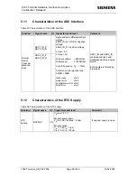
5.11
Characteristics of the ADC Interface
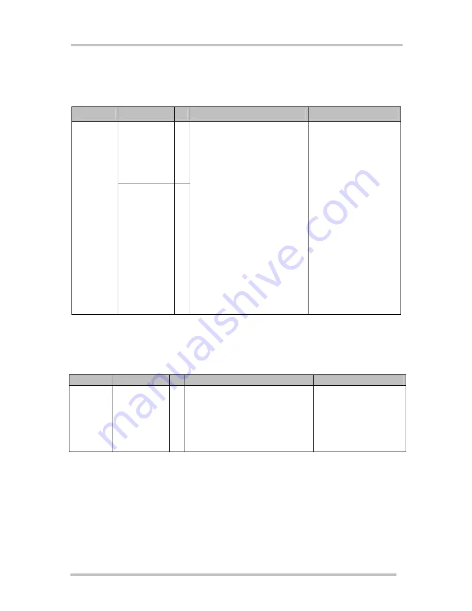
Table 37: Characteristics of the ADC interface
Function
Signal name
IO Signal form and level
Comment
ADC1_IN_P
ADC1_IN_N
Analog/
Digital
Converter
balanced
input
ADC2_IN_P
ADC2_IN_N
Sin
gle ended or differential input
voltage
ADCx_IN_N = GND or negative
voltage
ADCx_IN_P = positive voltage
VI min = 0V
VI max = 5V
Ri single ended
≈
600kOhm
Ri balanced
≈
1200kOhm
Cut-off-frequency, fg = 70Hz
Common-mode rejection ratio,
CMRR > 50dB
Inaccuracy ±1mV
Linear error
±1mV
Temperature error ±1mV
Burst e
rror ±1mV
ADC1_IN and ADC2_IN
are balanced lines and
multiplexed with an analog
switch.
Both inputs are filtered by
a low pass
5.12
Characteristics of the RTC Supply
Table 38: Characteristics of the RTC supply
Function
Signal name
IO Signal form and level
Comment
RTC
backup
BACKUP I/O
V
IN
max = 4.7V
Module power down
V
IN
min=2.6V at Imax = 25µA
Module active
V
IN
=<3.6V I
IN
= 0µA
V
IN
=>3.7V I
IN
= 25µA
If unused, keep pin open.


