15
7.3.2 Line deflection
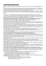
The final line transistor is driven by the transformer 5441, whose primary winding is driven by the transistor T7440
connected to the line drive output of IC7015 (pin 48).
The horizontal deflection stage is carried out in a conventional way, with the deflection transistor (T7445) and line
transformer (5445).
Beam current info (BCI) is present at C2460.
There are the following supply voltages obtained from line transformer (5545):
+25V : To supply frame deflection..
FF : The heather voltage is reduced by R3235/38 and 5201/02 (Diagram B) to obtain 6.3Veff at the CRT.
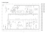
7.4 SOUND AMPLIFIER (Diagram C)
Sound amplifier is a Bridge Tied Load (BTL) amplifier short circuit protection, mute and stand by mode.
IC used can be TDA8941 for 14" and 17" models or TDA8943 for 20" and 21" models. TDA8944 is reserved for stereo
models (not explained in this manual).
- Supply (Vcc, SVR): Main supply (Vcc) is taken from +11V of Power Supply (C2540 diagram D). The IC creates
internally a half supply, present in SVR pin and decoupled by 10uF capacitor.
- Sound input (IN+): This amplifier has a differential input (IN+,IN-). Audio input is connected to IN+ decoupled by 220nF
capacitor (C2186) and IN- is decoupled to ground by other 220nF capacitor. To avoid oscillations there is a 1n5 capacitor
connected between both inputs.
- Mode input: This input is commanded by the µC and has three modes depending of the voltage level:
- Standby mode (Vmode=Vcc): Consumption is very low (used during stand by)
- Mute mode (2.5V<Vmode<Vcc): No sound output (used when the set is switched on/off, there is no signal, etc.)
- Operating mode: (Vmode<0.5V): Sound output present (normal operation).
- Sound output (OUT+/OUT-): Amplified sound is drived to the loudspeakers. Headphones output has been connected
in such a way that when headphones are connected, loudspeakers are switched off.
7.5 POWER SUPPLY (Diagram D)
Mains isolated switched mode power supply (SMPS), controlled by IC7514 (TDA4605) in variable frequency mode.
- Switching behaviour: The switching period is divided in on-time, when energy is extracted from the mains into the
primary winding (8-12 of 5525), off-time, when energy in the transformer is supplied to the loads via secondary windings
of 5525 and dead-time when no energy is extracted or supplied.
- Standby mode: Output voltages are present when the set is on stand by, due to standby is done cutting line deflection.
On-time is lower and power consumption is very low.
7.5.1 Primary side
- Degaussing: R3501 is a dual PTC (2 PTC’s in one housing). After switch on set, PTC is cold so low-ohmic and so
degaussing current is very high. After degaussing, PTC is heated so high-ohmic, so in normal operation degaussing
current is very low.
- Rectifier: Mains voltage is filtered by L5500, full wave rectified by diodes D6502-D6505 and smoothed by C2505 (300V
DC for 220V AC mains).
7.5.2 Control circuit (IC7514)
- Start up and supply (pin 6): When the set is switched on, a current via R3507 is applied to pin 6. When C2514 is
charged to 15V, the power supply starts and a current from pin 5 to T7525 is drived. T7525 and starts conduction and a
voltage across transformer windings is built up. The voltage across winding 4-2 is rectified by diode D6521 and used to
supply the IC on pin 6.
- Soft start (pin 7): The capacitor C2523 causes a slow increase of the duration of the output pulse during start up.
- IC output (pin 5): This output drives T7525. R3523 is a fuse resistor to protect IC from short circuits in T7525. D6516
limits the maximum voltage in T7525.
- Start conduction of T7525 (pin 8): A voltage proceeding from winding 4-2 is applied to this pin. The zero crossing
detector recognizes the complete discharge of the energy stored in the transformer core, in addition to a dead time
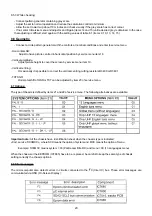
depending on C2508. This circuit guarantee that T7525 starts conduction at minimum Vds voltage (see fig 7.5).
- Primary current info (pin 2): Current primary winding is simulated by a pin 2 voltage.
- Output voltage info (pin 1): The voltage across winding 4-2 is rectified by diode D6515, divided by R3517, R3518 and
R3508 and applied to pin 1. Internal control voltage (Vcont) inversely proportional to Vpin1 is generated.


