background image


41110555 

Rev 1.0 

November 01, 2017 

23 

3.  Detailed Interface Specifications 

Note:  

If not specified, all electrical values are given for VBATT=3.7V and an operating temperature of 25°C. 


For standard applications, VBATT and VBATT_PA must be tied externally to the same power supply. 

For some specific applications, AirPrime HL77xx modules support separate VBATT and VBATT_PA 

connections if requirements below are fulfilled. 

3.1.  Power Supply 

The 

AirPrime HL77xx modules are

 supplied through the 

VBATT and VBATT_PA 

signals

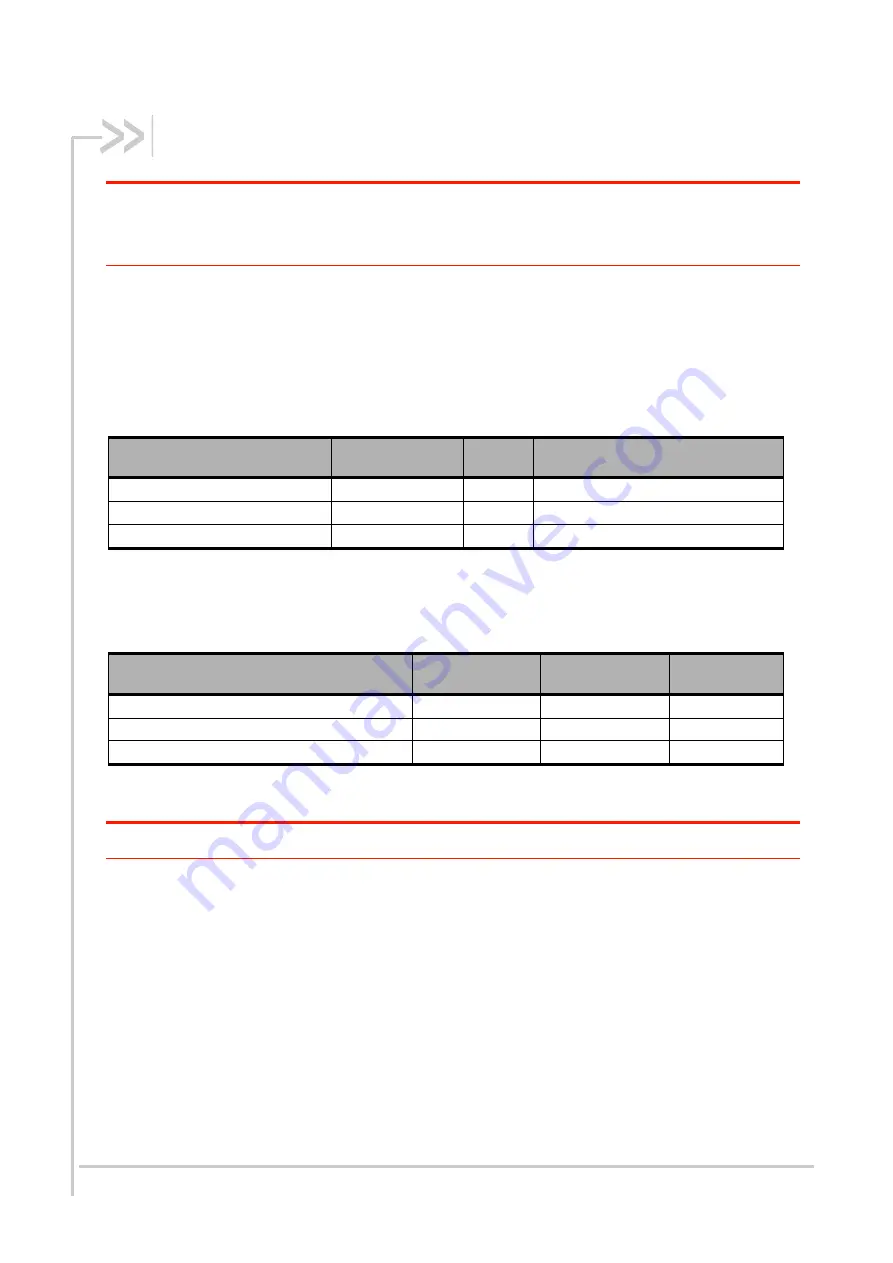
Refer to the following table for the pad description of the Power Supply interface. 

Table 7. 

Power Supply Pad Description 

Pad Number 

Signal Name 

I/O 

Description 

63 

VBATT 

Power supply (base band) 

61, 62 

VBATT_PA  

Power supply (radio frequency) 

37, 39, 48, 67-70, 167-234 

GND 


Ground 

 
Refer to the following table for the electrical characteristics of the Power Suppl

y

 interface. 

Table 8. 

Power Supply Electrical Characteristics 

Supply 

Minimum 

Typical 

Maximum 

VBATT voltage (V) 

3.2

1


3.7 

4.5 

VBATT_PA voltage (V) Full Specification 

3.2

1


3.7 

4.5 

VBATT_PA voltage (V) Extended Range 

2.8

2

 (TBC) 

3.7 

4.5 

1   

This value must be guaranteed during the burst 

2   

No guarantee of 3GPP performances over extended range 

Note:  

Load capacitance for VBATT is around 37µF ± 20% (TBC) embedded inside the module. 

Load capacitance for VBATT_PA is around 11µF ± 20% (TBC) embedded inside the module. 

Summary of Contents for AirPrime HL77 Series

Page 1: ...Product Technical Specification AirPrime HL77xx 41110555 1 0 November 01 2017...

Page 2: ...terfere with various onboard systems Note Some airlines may permit the use of cellular phones while the aircraft is on the ground and the door is open Sierra Wireless modems may be used at this time T...

Page 3: ...erra Wireless Inc or one of its subsidiaries Watcher is a registered trademark of NETGEAR Inc used under license Windows and Windows Vista are registered trademarks of Microsoft Corporation Macintosh...

Page 4: ...41110555 Rev 1 0 November 01 2017 4 Product Technical Specification Document History Version Date Updates 1 0 November 01 2017 Creation...

Page 5: ...DEFINITION 17 2 1 Pad Types 21 2 2 Pad Configuration Top View Through Module 22 3 DETAILED INTERFACE SPECIFICATIONS 23 3 1 Power Supply 23 3 2 Current Consumption 24 3 3 VGPIO 25 3 4 USIM Interface 2...

Page 6: ...M1 Application 41 5 7 EMC and ESD Guidelines for USIM1 Card 41 5 8 ESD Guidelines for USB 42 5 9 PWM 42 6 RELIABILITY SPECIFICATION TBC 44 6 1 Reliability Compliance 44 6 2 Reliability Prediction Mode...

Page 7: ...lative Timing for the PWM Output 34 Figure 9 Mechanical Drawing 37 Figure 10 Dimensions and Footprint Drawing 38 Figure 11 Voltage Limiter Example 40 Figure 12 PWR_ON_N Connection Example with Switch...

Page 8: ...Digital I O Electrical Characteristics 27 Table 18 GPIO Pad Description 28 Table 19 UART1 Pad Description 28 Table 20 PWR_ON_N Pad Description 29 Table 21 PWR_ON_N Electrical Characteristics 29 Table...

Page 9: ...Table 39 Life Stress Test 44 Table 40 Environmental Resistance Stress Tests 45 Table 41 Corrosive Resistance Stress Tests 45 Table 42 Thermal Resistance Cycle Stress Tests 46 Table 43 Mechanical Resi...

Page 10: ...ted Bands Connectivity RF Band Transmit Band Tx Receive Band Rx Maximum Output Power HL7718 HL7748 HL7749 LTE B2 1850 to 1910 MHz 1930 to 1990 MHz 23dBm 2dBm LTE B3 1710 to 1785 MHz 1805 to 1880 MHz 2...

Page 11: ...nection pads RF main interface Baseband signals connection Electrical Single or double supply voltage VBATT and VBATT_PA 3 2V 4 5V RF HL7718 Mono band LTE LTE B13 HL7748 Tri band LTE LTE B2 LTE B4 LTE...

Page 12: ...rage SMS sorting SMS concatenation SMS Status Report SMS replacement support SMS storing rules support of AT CNMI AT CNMA Connectivity Multiple cellular packet data profiles Sleep mode for minimum idl...

Page 13: ...DSP PMU Analog Baseband Embedded SIM LGA 146 PWR_ON SAW Filters USB Front End Module SAW PA Switch RX RAM Memory Peripherals Flash Memory SIM Switch Transceiver 26MHz VBATT_PA Figure 1 Architecture O...

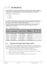
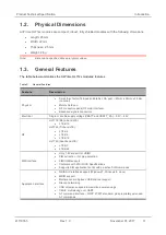
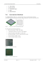
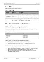
Page 14: ...de through the 146 Land Grid Array LGA pads on the bottom side of the PCB Figure 2 Mechanical Overview Top View and Bottom View The 146 pads have the following distribution 66 inner signal pads 1x0 5m...

Page 15: ...nvironmental Specifications The environmental specification for both operating and storage conditions are defined in the table below Table 4 Environmental Specifications Conditions Range Operating Cla...

Page 16: ...he market does not contain lead mercury cadmium hexavalent chromium polybrominated biphenyls PBB or polybrominated diphenyl ethers PBDE 1 8 4 Disposing of the Product This electronic product is subjec...

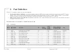
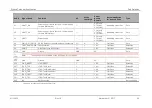
Page 17: ...as not connected or reserved should not be used Table 5 Pin Definition Pad Signal Name Function I O Active Low High Power Supply Domain Recommendation for Unused Pads Type 1 GPIO1 General purpose inp...

Page 18: ...onnected Reserved for future use Not connected 21 NC Not Connected Not connected 22 GNSS_FREQ_OUT 26MHz System Clock Output O 1 8V Left Open Extension 23 32K_CLKOUT 32 768kHz System Clock Output O 1 8...

Page 19: ...Open Extension 45 VGPIO GPIO voltage output O 1 8V Left Open Core 46 GPIO6 General purpose input output I O 1 8V Left Open Core 47 NC Not Connected Reserved for future use Left Open Not connected 48 G...

Page 20: ...ection General purpose input output I O H 1 8V Left Open Core 65 FAST_SHUTDOWN Fast Shutdown I L 1 8V Left Open Extension 66 GPIO5 General purpose input output I O 1 8V Left Open Extension 67 70 GND G...

Page 21: ...n 2 1 Pad Types Table 6 Pad Type Codes Type Definition I Digital Input O Digital Output I O Digital Input Output L Active High H Active Low T Tristate T PU Tristate with pull up enabled T PD Tristate...

Page 22: ...0 225 224 223 222 203 176 186 209 208 207 206 205 204 177 185 184 183 182 181 180 179 178 236 237 238 239 240 241 242 GND GPIO5 FAST_SHUTDOWN UIM1_DET GPIO3 VBATT VBATT_PA VBATT_PA NC PWR_ON_N PWM0 NC...

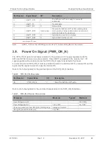
Page 23: ...Supply interface Table 7 Power Supply Pad Description Pad Number Signal Name I O Description 63 VBATT I Power supply base band 61 62 VBATT_PA I Power supply radio frequency 37 39 48 67 70 167 234 GND...

Page 24: ...PSM mode 100 TBC TBD A Table 10 Current Consumption Parameter Band Frequency Typical Unit LTE in communication mode TX Max Pout 23dBm BW 10Mhz RMC mode 4RB_DL 6RB_UL B3 1810 MHz 290 mA 1843 MHz 285 m...

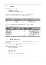
Page 25: ...nimum Typical Maximum Remarks Voltage level V 1 7 1 8 1 9 Both active mode and sleep mode Current capability Active Mode mA TBD Power management support up to TBD mA output in Active mode Current capa...

Page 26: ...section 5 6 USIM1 Application for a USIM application example 3 4 1 UIM1_DET UIM1_DET is used to detect and notify the application about the insertion and removal of a USIM device in the USIM socket c...

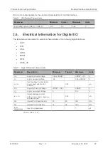
Page 27: ...l interfaces UART PCM JTAG GPIOs RESET PWM WAKE_UP Table 17 Digital I O Electrical Characteristics Parameter Description Minimum Typical Maximum Units VIH Logic High Input Voltage 0 85 x VDDIO VDDIO 0...

Page 28: ...The main serial link UART1 is used for communication between the AirPrime HL77xx modules and a PC or host processor It consists of a flexible 8 wire serial interface that complies with RS 232 interfa...

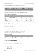
Page 29: ...nt 1 8V supply regulator inside the AirPrime HL77xx module via a pull up resistor Once VBATT is supplied to the module this 1 8V supply regulator will be enabled and so the PWR_ON_N signal is by defau...

Page 30: ...use AT command AT CPOF or AT CPWROFF 3 10 Reset Signal RESET_IN_N To reset the module a low level pulse must be sent on the RESET_IN_N pad for 20ms TBC This action will immediately restart the AirPrim...

Page 31: ...Cs ranging from 0 to 1 8V Typical ADC use is for monitoring external voltage wherein an application is used to safely power OFF an external supply in case of overvoltage Refer to the following table f...

Page 32: ...on Pad Number Signal Name I O I O Type Description 44 DEBUG_TX O 1 8V Debug Transmit Data 51 DEBUG_RX I 1 8V Debug Receive Data According to module view Note It is strongly recommended to provide acce...

Page 33: ...AirPrime HL77xx modules provide one WAKE UP signal The WAKE UP signal is used to wake the system up from ultra low power modes from OFF or Sleep modes FAST_SHUTDOWN or after a software power off This...

Page 34: ...r Signal Name I O I O Type Description 65 FAST_SHUTDOWN I 1 8V Shuts down the module without deregistration from the network Refer to the following table for the electrical characteristics of the FAST...

Page 35: ...terface of the AirPrime HL77xx modules allow the transmission of RF signals This interface has a 50 nominal impedance 3 18 1 RF Connection A 50 with maximum VSWR 1 1 1 and 0 5dB loss RF track is recom...

Page 36: ...hnical Specification Detailed Interface Specifications Table 37 Typical RX Sensitivity LTE Band dBm 15kHz dBm 1 4MHz 3GPP Limit dBm 2 126 107 4 100 3 3 126 107 4 99 3 4 125 5 106 9 102 3 12 125 5 106...

Page 37: ...41110555 Rev 1 0 November 01 2017 37 4 Mechanical Drawings Figure 9 Mechanical Drawing...

Page 38: ...41110555 Rev 1 0 November 01 2017 38 Product Technical Specification Mechanical Drawings Figure 10 Dimensions and Footprint Drawing...

Page 39: ...PWR_ON_N is internally pulled up with 1M an open collector or open drain transistor must be used for ignition 5 2 Module Switch Off AT commands AT CPOF and AT CPWROFF enables the user to properly swi...

Page 40: ...module s power supply lines so that VBATT and VBATT_PA signal pads will never receive a voltage surge over 4 5V The voltage limiter can be as simple as a Zener diode with decoupling capacitors as sho...

Page 41: ...rs must be added according to the drawing below as close as possible to the UIM1 card connectors on UIM1_CLK UIM1_RESET UIM1_VCC UIM1_DATA and UIM1_DET signals to avoid EMC issues and to comply with t...

Page 42: ...r USB Sierra Wireless recommends using the following components FIL400 90 DLP0NSN900HL2L EMC filter D400 RCLAMP0503N or ESD5V3U2U 03LRH ESD diode 5 9 PWM Refer to the following figures for examples of...

Page 43: ...oduct Technical Specification Design Guidelines Figure 18 Example of a BUZZER Driven by the PWM0 Output The recommended MOS transistor to use for T1 is the RUM003N02 from ROHM and the recommended diod...

Page 44: ...nts Table 38 Standards Conformity Abbreviation Definition IEC International Electro technical Commission ISO International Organization for Standardization 6 2 Reliability Prediction Model 6 2 1 Life...

Page 45: ...and 2 minutes OFF Duration 3 days Resistance to Heat Test RH Standard IEC 680068 2 2 Test Bb Special conditions Temperature 85 C Temperature variation 1 C min Operating conditions Powered ON with a po...

Page 46: ...on 3 0 6 C min Operating conditions Powered ON for 15 minutes during each 3 hours ramp up and 3 hours ramp down in middle for every cycle Duration 21 days 6 2 4 Thermal Resistance Cycle Stress Tests T...

Page 47: ...ycle Number of Sweep 20 sweeps axis Sweep direction X Y Z Operating conditions Un powered Duration 2 days Random Vibration Test RVT Standard IEC 60068 2 64 Test Fh Special conditions Frequency range 1...

Page 48: ...dard JESD22 A114 JESD22 A115 JESD22 C101 Special conditions HBM Human Body Model 1KV Class 1C MM Machine Model 200V CDM Charged Device Model 250V Class II Operating conditions Powered Duration 3 days...

Page 49: ...ximum antenna gain including cable loss in a mobile only exposure condition must not exceed For HL7718 2 dBi in Band 13 For HL7748 9 0 dBi in Band 2 6 0 dBi in Bands 4 and 12 3 The HL7718 and HL7748 m...

Page 50: ...nics micro controllers etc may degrade the reception performances The GSM GPRS connector is intended to be directly connected to a 50 antenna and no matching is needed 5 A label must be affixed to the...

Page 51: ...el Name Description Part Number HL7718 HL7718 embedded module Contact Sierra Wireless for the latest SKU HL7748 HL7748 embedded module Contact Sierra Wireless for the latest SKU HL7749 HL7749 embedded...

Page 52: ...communications Standards Institute FDMA Frequency division multiple access GAGAN GPS aided geo augmented navigation GLONASS Global Navigation Satellite System GND Ground GNSS Global Navigation Satelli...

Page 53: ...ubscriber Identification Module SMD Surface Mounted Device Design SPI Serial Peripheral Interface SW Software PSRAM Pseudo Static RAM TBC To Be Confirmed TBD To Be Defined TP Test Point TX Transmit TY...

Reviews: