Copyright
c
2016, SiFive Inc. All rights reserved.
43
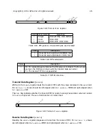
Value
Description
0
Data is sampled on the leading edge of SCK and shifted on the trailing edge of SCK
1
Data is shifted on the leading edge of SCK and sampled on the trailing edge of SCK
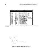
Table 13.3: Serial clock phase.
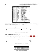
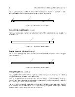
Chip Select ID Register (
csid
)
The
csid
register encodes the index of the CS pin to be toggled by hardware chip select control.
The reset value is
0
.
csid
31
0
Figure 13.3: Format of
csid
register.
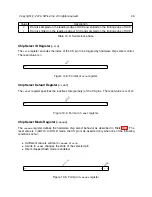
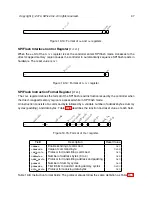
Chip Select Default Register (
csdef
)
The
csdef
register specifies the inactive state (polarity) of the CS pins. The reset value is
0xFFFF
.
csdef
31
0
Figure 13.4: Format of
csdef
register.
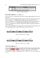
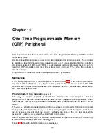
Chip Select Mode Register (
csmode
)
The
csmode
register defines the hardware chip select behavior as described in Table 13.4. The
reset value is
0
(AUTO). In HOLD mode, the CS pin is de-asserted only when one of the following
conditions occur:
•
A different value is written to
csmode
or
csid
.
•
A write to
csdef
changes the state of the selected pin.
•
Direct-mapped flash mode is enabled.
R
eserve
d
31
2
mode
1
0
Figure 13.5: Format of
csmode
register.
Summary of Contents for E300
Page 1: ...SiFive E300 Platform Reference Manual Version 1 0 1 c SiFive Inc ...
Page 2: ...2 SiFive E300 Platform Reference Manual Version 1 0 1 ...
Page 4: ...ii SiFive E300 Platform Reference Manual Version 1 0 1 ...
Page 12: ...4 SiFive E300 Platform Reference Manual Version 1 0 1 ...
Page 14: ...6 SiFive E300 Platform Reference Manual Version 1 0 1 ...
Page 22: ...14 SiFive E300 Platform Reference Manual Version 1 0 1 ...
Page 32: ...24 SiFive E300 Platform Reference Manual Version 1 0 1 ...
Page 40: ...32 SiFive E300 Platform Reference Manual Version 1 0 1 ...
Page 56: ...48 SiFive E300 Platform Reference Manual Version 1 0 1 ...
Page 60: ...52 SiFive E300 Platform Reference Manual Version 1 0 1 ...

