background image

Chapter 1

Introduction

The E300 platform is the first member of SiFive’s Freedom Everywhere family of customizable
RISC-V SoCs. By combining a highly configurable base platform with customer-specific hardware
extensions, the Freedom Everywhere family provides low-NRE and rapid time-to-market solutions
for performance, cost, and power-sensitive embedded and IoT markets.

Each E300 SoC includes a SiFive E3 series RISC-V Coreplex with integrated instruction and data
memories, a platform-level interrupt controller, on-chip debug unit, and an extensive selection of
peripheral devices. This manual should be read together with the E3 Coreplex manual.

All aspects of the base E300 platform can be flexibly configured. In addition, the platform can be
readily extended with customer-specific instruction-set extensions, custom coprocessors, custom
accelerators, custom I/O, and custom always-on blocks. The resulting application-specific E300
SoC is optimized for manufacture in a TSMC 180nm process, and delivered as packaged tested
parts by SiFive.

Block Diagram

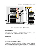
Figure 1.1 shows the top-level block diagram of the E300 platform. The heart of the current
E300 platform is an E31 Coreplex, which contains an E31 RISC-V processor, instruction and data
memories, the platform-level interrupt controller (PLIC), a central DMA controller, and a debug
module.

Configurable E31 RISC-V Coreplex

The configurable E31 RISC-V Coreplex provides a high-performance single-issue in-order 32-bit
execution pipeline, with a peak sustained execution rate of one instruction per clock cycle. The
Freedom E300 platform supports most configuration options of the E31 core as described in the
E3 Coreplex manual, except for the following:

Where present, the instruction cache line size is 32 bytes.

The data cache is not supported.

The E3 Coreplex exports two TileLink attachments; a TileLink master port which can be used to
attach a custom accelerator, and a TileLink slave port to drive the platform bus. Both ports support
32-byte burst accesses over a 32-bit datapath.

1

Summary of Contents for E300

Page 1: ...SiFive E300 Platform Reference Manual Version 1 0 1 c SiFive Inc ...

Page 2: ...2 SiFive E300 Platform Reference Manual Version 1 0 1 ...

Page 3: ...bil ity fitness for a particular purpose and non infringement SiFive does not assume any liability rising out of the application or use of any product or circuit and specifically disclaims any and all liability including without limitation indirect incidental special exemplary or consequential damages SiFive reserves the right to make changes without further notice to any products herein Release I...

Page 4: ...ii SiFive E300 Platform Reference Manual Version 1 0 1 ...

Page 5: ...ower Management 3 1 9 Debug Support 3 1 10 Software Tools 3 2 E300 Platform Memory Map 5 3 E300 Power Modes 7 3 1 Run Mode 7 3 2 Wait Mode 7 3 3 Sleep Mode 7 4 E300 Clock Generation 9 4 1 Clock Generation Overview 9 4 2 Internal Trimmable Programmable 72 MHz Oscillator HFROSC 9 4 3 External 16 MHz Crystal Oscillator HFXOSC 11 4 4 Internal High Frequency PLL HFPLL 11 4 5 PLL Output Divider 13 4 6 I...

Page 6: ...am 19 6 4 Initiate Sleep Sequence Register pmusleep 20 6 5 Wakeup Signal Conditioning 21 6 6 PMU Interrupt Enables pmuie and Wakeup Cause pmucause 21 6 7 Memory Map 22 7 E300 Power Reset Clock Interrupt PRCI Control and Status Registers 23 7 1 PRCI Address Space Usage 23 8 E300 Watchdog Timer WDT 25 8 1 Watchdog Count Register wdogcount 25 8 2 Watchdog Clock Selection 26 8 3 Watchdog Configuration...

Page 7: ...smit Data Register txdata 38 12 4 Receive Data Register rxdata 38 12 5 Transmit Control Register txctrl 38 12 6 Receive Control Register rxctrl 39 12 7 Interrupt Registers ip and ie 39 12 8 Baud Rate Divisor Register div 39 13 Serial Peripheral Interface SPI 41 13 1 SPI Overview 41 13 2 Memory Map 41 13 3 Serial Clock Divisor Register sckdiv 41 13 4 Serial Clock Mode Register sckmode 42 13 5 Chip ...

Page 8: ...rammed I O Sequencing 51 14 4 Read sequencer control register otp rsctrl 51 15 E300 Pulse Width Modulation PWM Peripheral 53 15 1 PWM Overview 53 15 2 PWM Memory Map 53 15 3 PWM Count Register pwmcount 53 15 4 PWM Configuration Register pwmcfg 54 15 5 PWM Compare Registers pwmcmp0 pwmcmp3 55 15 6 Deglitch and Sticky circuitry 56 15 7 Generating Left or Right Aligned PWM Waveforms 56 15 8 Generatin...

Page 9: ...on specific E300 SoC is optimized for manufacture in a TSMC 180nm process and delivered as packaged tested parts by SiFive Block Diagram Figure 1 1 shows the top level block diagram of the E300 platform The heart of the current E300 platform is an E31 Coreplex which contains an E31 RISC V processor instruction and data memories the platform level interrupt controller PLIC a central DMA controller ...

Page 10: ... SRAM OTP FPU Power Management Figure 1 1 Top Level Block Diagram of the E300 platform Custom Accelerators Custom autonomous accelerators can be added to provide application specific processing The custom accelerators can directly access on chip memories and peripheral devices and can gen erate and receive interrupts from the platform level interrupt controller On Chip Memory The on chip memory sy...

Page 11: ...esponse Always On Block and Power Management E300 SoCs can be configured with active power management to reduce leakage current in sleep mode The Always On Block AON supports low power sleep with wakeup from an internal real time clock interrupt or external I O stimulus or custom always on circuitry Debug Support Each E300 system includes extensive platform level debug facilities including hardwar...

Page 12: ...4 SiFive E300 Platform Reference Manual Version 1 0 1 ...

Page 13: ...PRCI 32 KiB 0x1001 0000 0x1001 0FFF On chip OTP control 0x1001 1000 0x1001 1FFF On chip eFlash control 0x1001 2000 0x1001 2FFF GPIO0 0x1001 3000 0x1001 3FFF UART0 0x1001 4000 0x1001 4FFF QSPI0 0x1001 5000 0x1FFF FFFF Additional Peripherals 256MiB 0x2000 0000 0x3FFF FFFF Off chip QSPI0 flash read 512 MiB 0x4000 0000 0x7FFF FFFF Additional I O or RAM 1 GiB 0x8000 0000 0x8001 FFFF Instruction and Dat...

Page 14: ...6 SiFive E300 Platform Reference Manual Version 1 0 1 ...
Page 15: ... to determine the correct course of action Sleep Mode Sleep mode is entered by writing to a memory mapped register pmusleep in the power management unit PMU The pmusleep register is protected by the pmukey register which must be written with a defined value before writing to pmusleep The PMU will then execute a power down sequence to turn off power to the processor and main pads All volatile state...

Page 16: ...atform Reference Manual Version 1 0 1 always initially runs from the HFROSC at the default setting and must reconfigure clocks to run from an alternate clock source HFXOSC or PLL or at a different setting on the HFROSC ...

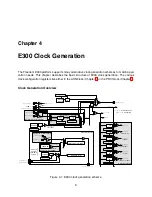
Page 17: ...G tck 16MHz hfroscout 1 125 72MHz lfxoscin lfxoscout 32 768kHz hfxoscin hfxoscout 16MHz LFRCOSC lfrcoscout 30 60kHz pllcfg jtagclk N plloutdiv coreclk N spiclkcfg spiclk 8 16 baud rate N uartclkcfg uartclk 25MHz 125MHz N enetclkcfg enetclk N usbclkcfg usbclk 60MHz hfclk N hyperclkcfg hyperclk 166MHz N i2sclkcfg i2sclk 1 536MHz 1 4112MHz pllrefsel 1 0 jtagclk is selected when psdscanen is asserted ...

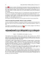
Page 18: ...9 21 20 16 15 6 5 0 hfroscrdy hfroscen 0 hfrosctrim 0 hfroscdiv 1 1 9 5 10 6 Table 4 1 The HFROSC config register hfrosccfg The frequency can be adjusted in software using a 5 bit trim value in the hfrosctrim The trim value from 0 31 adjusts which tap of the variable delay chain is fed back to the start of the ring A value of 0 corresponds to the longest chain and slowest frequency while higher va...

Page 19: ... bypass The HFXOSC is controlled via the memory mapped hfxosccfg register 31 30 29 0 hfxoscrdy hfxoscen 0 1 1 30 Table 4 2 The HFXOSC config register hfxoscccfg The hfxoscen bit turns on the crystal driver and is set after wakeup reset but can be cleared to turn off the crystal driver and reduce power consumption The hfxoscrdy bit indicates if the crystal oscillator output is ready for use The hfx...

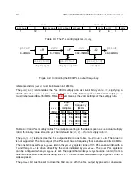
Page 20: ...Max Min Max 6 64 128 384 768 8 48 96 384 768 10 39 76 390 760 12 32 64 384 768 Table 4 4 Valid PLL multiply ratios The multiplier setting in the table is given as the actual multiply ratio the binary value stored in pllf field should be M 2 1 for a multiply ratio M The pllq 1 0 field encodes the PLL output divide ratio as follow 01 2 10 4 11 8 The value 00 is not supported The final output of the ...

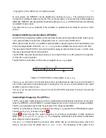
Page 21: ...F capacitor across the VDDPLL VSSPLL supply pins The VSSPLL pin should not be connected to board VSS PLL Output Divider The plloutdiv register controls a clock divider that divides the output of the PLL 0 31 9 p l l o u t d i v b y 1 8 0 7 6 p l l o u t d i v 5 0 Figure 4 3 PLL Output Divider Register plloutdiv If the plloutdivby1 bit is set the PLL output clock is passed through undivided If pllo...

Page 22: ...14 SiFive E300 Platform Reference Manual Version 1 0 1 ...

Page 23: ... domain crossing VCDC bridges TileLink between the two power and clock domains AON Reset Unit An AON reset is the widest reset on an E300 system and resets all state except for the JTAG debug interface An AON reset can be triggered by an on chip power on reset POR circuit when power is first applied to the AON domain an external active low reset pin erst n or expiration of the watchdog timer wdogr...

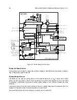
Page 24: ...dlfaltclk psdcorerst_n psdhfclkrst_n psdlfclksel 1 0 lfroscrst 0 Reset Synchronizer aonrst Reset Cause aonrst psdaonrstout Figure 5 1 E300 Always On Domain Power On Reset Circuit This optional circuit holds it s output low until the voltage in the AON block rises above a design time configurable preset threshold External Reset Circuit The E300 can be reset by pulling down on the external reset pin...

Page 25: ...keup from sleep mode or timer interrupts during normal operation The Real Time Clock is described in detail in Chapter 9 Backup Registers The backup register provide a configurable number of 32 bit data registers that hold state during sleep The FE310 G000 has 16 32 bit backup registers The backup registers are described in detail in Chapter 10 Power Management Unit PMU The power management unit P...

Page 26: ... Clock Registers 0x1000 0044 Reserved 0x1000 0048 rtclo 0x1000 004C rtchi 0x1000 0050 rtcs 0x1000 0054 Reserved 0x1000 0058 Reserved 0x1000 005C Reserved 0x1000 0060 rtccmp 0x1000 0070 lfrosccfg AON Clock Configuration Registers 0x1000 0080 backup0 Backup Registers 0x1000 0084 backup1 0x1000 00FC backup31 0x1000 0100 PMU wakeup program memory Power Management Unit 0x1000 0120 PMU sleep program mem...

Page 27: ...mukey register has one bit of state To prevent spurious sleep or PMU program modification all writes to PMU registers must be preceded by an unlock operation to the pmukey register loca tion which sets pmukey The value 0x51F15E must be written to the pmukey register address to set the state bit before any write access to any other PMU register The state bit is reset at AON reset and after any writ...

Page 28: ...e d 4 d e l a y 3 0 Figure 6 2 PMU instruction format At power on reset the PMU program memories are reset to conservative defaults Table 6 1 shows the default wakeup program and Table 6 2 shows the default sleep program Index Value Meaning 0 0x1f0 Assert all resets and enable all power supplies 1 0x0f8 Idle 28 cycles then deassert hfclkrst 2 0x030 Deassert corerst and padrst 3 7 0x030 Repeats Tab...

Page 29: ...ch events can wake the MOFF block from sleep The awakeup bit indicates that the awakeup pin can rouse MOFF The dwakeup bit indicates that a logic 0 on the dwakeup n pin can rouse MOFF The rtc bit indicates that the RTC comparator can rouse MOFF R e s e r v e d 31 4 a w a k e u p 3 d w a k e u p 2 r t c 1 R e s e r v e d 0 Figure 6 3 Format of pmuie register Following a wakeup the pmucause register...

Page 30: ...ion 4 0x114 pmuwakeupi5 Wakeup program instruction 5 0x118 pmuwakeupi6 Wakeup program instruction 6 0x11c pmuwakeupi7 Wakeup program instruction 7 0x120 pmusleepi0 Sleep program instruction 0 0x124 pmusleepi1 Sleep program instruction 1 0x128 pmusleepi2 Sleep program instruction 2 0x12c pmusleepi3 Sleep program instruction 3 0x130 pmusleepi4 Sleep program instruction 4 0x134 pmusleepi5 Sleep progr...

Page 31: ... the name The PRCI registers are generally only made visible to machine mode software The AON block contains registers with similar functions but only for the AON block units PRCI Address Space Usage Table 7 1 shows the memory map for PRCI on SiFive systems Address Description 0x1000 8000 hfrosccfg Clock Configuration Registers 0x1000 8004 hfxosccfg 0x1000 8008 pllcfg 0x1000 800c plloutdiv 0x1000 ...

Page 32: ...24 SiFive E300 Platform Reference Manual Version 1 0 1 ...
Page 33: ...a preset threshold else it will trigger a full power on reset To prevent errant code from resetting the counter the WDT registers can only be updated by presenting a WDT key sequence wdogcmp wdogcfg wdogcmpip wdogclk aonrst wdogcount wdogs wdogscale Wdog TileLink wdogfeed reset wdogrst aonrst en wdogclk wdogkey corerst Synch wdogzerocmp wdogrsten wdogenalways wdogencoreawake Figure 8 1 E300 Watchd...

Page 34: ...watchdog counter increments if the processor core is not asleep The WDT uses the corerst signal from the wakeup sequencer to know when the core is sleeping The counter increments by one each cycle only if any of the enabled conditions are true The wdogen bits are reset on AON reset The 4 bit wdogscale field scales the watchdog counter value before feeding it to the comparator The value in wdogscal...

Page 35: ...The value 0x51F15E must be written to the wdogkey register address to set the state bit before any write access to any other watchdog register The state bit is reset at AON reset and after any write to a watchdog register Watchdog registers may be read without setting wdogkey Watchdog Feed Address wdogfeed After a successful key unlock the watchdog can be fed using a write of the value 0xD09F00D t...

Page 36: ...dog re sets wdogrsten 0 and enabling auto zeroing of the count register when the comparator fires wdogzerocmp 1 The sticky single bit wdogcmpip register captures the comparator output and holds it to provide an interrupt pending signal The wdogcmpip register resides in bit 28 of the wdogcfg register and can be read and written over TileLink to clear down the interrupt ...

Page 37: ...0 Real Time Clock RTC Count Registers rtchi rtclo The real time counter is based around the rtchi rtclo register pair which increment at the low frequency clock rate when the RTC is enabled The rtclo register holds the low 32 bits of the RTC while rtchi holds the upper 16 bits of the RTC value The total 48 bit counter width ensures there will no counter rollover for over 270 years assuming a 32 76...

Page 38: ...ue of 0 in rtcscale indicates no scaling and rtcs would then be equal to rtclo The maximum value of 15 in rtcscale corresponds to dividing the clock rate by 215 so for an input clock of 32 768 kHz the LSB of rtcs will increment once per second The value of rtcs is memory mapped and can be read as a single 32 bit register over the AON TileLink bus The rtccmpip interrupt pending bit is read only RTC...

Page 39: ... Backup Registers The backup registers live in the Always On domain and provide a place to store critical data during sleep Each register is 32 bits wide and the number of backup registers is a configurable option 31 ...

Page 40: ...32 SiFive E300 Platform Reference Manual Version 1 0 1 ...
Page 41: ... has been designed to only require naturally aligned 32 bit memory accesses Input Output Values The same port register can be configured on a bitwise fashion to represent either inputs or out puts as set by the direction register Writing to the port register will update the bits regardless of the tristate value Reading the port register will return the written value Reading the value register will...

Page 42: ...t Shown Low Power Clamping Wake on Interrupt Logic IOF Signal Derivation D Q HIGH_IP D Q LOW_IP D Q RISE_IP D Q FALL_IP IOF_IVAL D Q HIGH_IE D Q LOW_IE D Q RISE_IE D Q FALL_IE INTERRUPT DS IOF1_OE IOF0_OVAL IOF0_OE D Q DS PUE D Q IE IVAL OVAL DS OE IE IE Q D OUT_XOR Figure 11 1 Structure of a single GPIO Pin with Control Registers This structure is repeated for each pin ...

Page 43: ...set to 0 Once the interrupt is pending it will remain set until a 1 is written to the ip register at that bit The interrupt pins may be routed to the PLIC or directly to local interrupts Internal Pull Ups When configured as inputs each pin has an internal pull up which can be enabled by software At reset all pins are set as inputs and pull ups are disabled Drive Strength When configured as output ...

Page 44: ...tware registers are fixed in the hardware on a per IOF basis Those that are not controlled by the hardware continue to be controlled by the software registers If there is no IOFx for a pin configured with IOFx the pin reverts to full software control Behavior During Sleep Mode ...

Page 45: ...g per bit The UART peripheral does not support hardware flow control or other modem control signals or synchronous serial data tranfesrs Memory Map The memory map for the UART control registers is shown in Table 12 1 The UART memory map has been designed to only require naturally aligned 32 bit memory accesses Address Name Description 0x000 txdata Transmit data register 0x004 rxdata Receive data r...

Page 46: ...g the rxdata register dequeues a character from the receive FIFO and returns the value in the data field The empty flag indicates if the receive FIFO was empty when set the data field does not contain a valid character Writes to rxdata are ignored e m p t y 31 0 30 8 d a t a 7 0 Figure 12 2 Format of rxdata register Transmit Control Register txctrl The read write txctrl register controls the opera...

Page 47: ...s are enabled ie is reset to 0 The txwm condition becomes raised when the number of entries in the transmit FIFO is strictly less than the count specified by the txcnt field of the txctrl register The pending bit is cleared when sufficient entries have been enqueued to exceed the watermark The rxwm condition becomes raised when the number of entries in the receive FIFO is strictly greater than the...

Page 48: ...6 250000 64 250000 0 200 31250 6400 31250 0 200 115200 1736 115207 0 0064 200 250000 800 250000 0 200 1843200 109 1834862 0 45 384 31250 12288 31250 0 384 115200 3333 115212 0 01 384 250000 1536 250000 0 384 1843200 208 1846154 0 16 Table 12 2 Common baud rates MIDI 31250 DMX 250000 and required divide values to achieve them with given bus clock frequencies The divide values are one greater than t...

Page 49: ...he external SPI flash device supports the common Win bond Numonyx serial read 0x03 command Sequential accesses are automatically combined into one long read command for higher performance The fctrl register controls switching between the memory mapped and programmed I O modes While in programmed I O mode memory mapped reads do not access the external SPI flash device and instead return 0 immediate...

Page 50: ... format 0x070 ie SPI interrupt enable 0x074 ip SPI interrupt pending Table 13 1 Register offsets within the SPI memory map Registers marked are present only on controllers with the direct map flash interface i e SPI0 R e s e r v e d 31 12 d i v 11 0 Figure 13 1 Format of sckdiv register Serial Clock Mode Register sckmode The sckmode register defines the serial clock polarity and phase Tables 13 2 ...

Page 51: ...t of csid register Chip Select Default Register csdef The csdef register specifies the inactive state polarity of the CS pins The reset value is 0xFFFF c s d e f 31 0 Figure 13 4 Format of csdef register Chip Select Mode Register csmode The csmode register defines the hardware chip select behavior as described in Table 13 4 The reset value is 0 AUTO In HOLD mode the CS pin is de asserted only when...

Page 52: ...riod delay is implicit The reset value is 0x01 The intercs field specifies the minimum CS inactive time between de assertion and assertion The reset value is 0x01 The interxfr field specifies the delay between two consecutive frames without de asserting CS This is applicable only when sckmode is HOLD or OFF The reset value is 0x00 R e s e r v e d 31 24 s c k c s 23 16 R e s e r v e d 15 8 c s s c ...

Page 53: ...s driven with the transmit data as normal 1 Tx The receive FIFO is not populated Table 13 7 SPI I O direction Transmit Data Register txdata Writing to the txdata register loads the transmit FIFO with the value contained in the data field For fmt len 8 values should be left aligned when fmt endian MSB and right aligned when fmt endian LSB The full flag indicates whether the transmit FIFO is ready t...

Page 54: ...which the Rx FIFO watermark interrupt triggers The reset value is 0 R e s e r v e d 31 3 r x m a r k 2 0 Figure 13 12 Format of rxmark register Interrupt Registers ie and ip The ie register controls which SPI interrupts are enabled and ip is a read only register indicating the pending interrupt conditions ie is reset to zero The txwm condition becomes raised when the number of entries in the trans...

Page 55: ...ruction consists of a command byte followed by a variable number of address bytes dummy cycles padding and data bytes Table 13 8 describes the function and reset value of each field p a d c o d e 31 24 c m d c o d e 23 16 R e s e r v e d 15 d a t a p r o t o 13 12 a d d r p r o t o 11 10 c m d p r o t o 9 8 p a d c n t 7 4 a d d r l e n 3 1 c m d e n 0 Figure 13 15 Format of ffmt register Field De...

Page 56: ...48 SiFive E300 Platform Reference Manual Version 1 0 1 ...
Page 57: ...it memory accesses The OTP controller also contains a read sequencer which exposes the OTP s contents as a read execute only memory mapped device Programmed I O lock register otp lock The otp lock register supports synchronization between the read sequencer and the programmed I O interface When the lock is clear memory mapped reads may proceed When the lock is set memory mapped reads do not access...

Page 58: ...voltage regulator control 0x1c otp mpp OTP write voltage charge pump control 0x20 otp vrren OTP read voltage enable 0x24 otp vppen OTP write voltage enable 0x28 otp a OTP device address 0x2c otp d OTP device data input 0x30 otp q OTP device data output 0x34 otp rsctrl OTP read sequencer control Table 14 1 SiFive OTP Register Offsets Only naturally aligned 32 bit memory accesses are supported la t0...

Page 59: ...ase a read pulse phase and a read access phase The duration of these phases in terms of controller clock cycles is set by a programmable clock divider The divider is controlled by the otp rsctrl register the layout of which is shown in Figure 14 2 The number of clock cycles in each phase is given by 2scale and the width of each phase may be optionally scaled by 3 That is the number of controller c...

Page 60: ...52 SiFive E300 Platform Reference Manual Version 1 0 1 ...
Page 61: ...be provided in different comparator precisions up to 16 bits with the version described here having the full 16 bits To support clock scaling the pwmcount register is 15 bits wider than the comparator precision cmpwidth PWM Memory Map The memory map for the PWM peripheral is shown in Table 15 1 PWM Count Register pwmcount The PWM unit is based around a counter held in pwmcount The counter can be r...

Page 62: ... c m p 1 c e n t e r 17 p w m c m p 0 c e n t e r 16 R e s e r v e d 15 14 p w m e n o n e s h o t 13 p w m e n a l w a y s 12 R e s e r v e d 11 p w m d e g l i t c h 10 p w m z e r o c m p 9 p w m s t i c k y 8 R e s e r v e d 7 4 p w m s c a l e 3 0 Figure 15 2 PWM configuration register pwmcfg The pwmcfg register contains various control and status information regarding the PWM peripheral as s...

Page 63: ...ck rate by 215 so for an input bus clock of 16 MHz the LSB of pwms will increment at 488 3 Hz The value of pwms is memory mapped and can be read as a single cmpwidth bit value over the TileLink bus The pwmzerocmp bit if set causes the PWM counter pwmcount to be automatically reset to zero one cycle after the pwms counter value matches the compare value in pwmcmp0 This is normally used to set the p...

Page 64: ...sed as a regular PWM edge otherwise If pwmdeglitch is set but pwmzerocmp is clear the deglitch circuit is still operational but is now trig gered when pwms contains all 1s and will cause a carry out of the high bit of the pwms incrementer just before the counter wraps to zero The pwmsticky bit will disallow the pwmcmpXip registers from clearing if they re already set and is used to ensure interrup...

Page 65: ...ic duty cycle as shown in Figure 15 6 The pwmcmpXcenter bit changes the comparator to compare with the bitwise inverted pwms value whenever the MSB of pwms is high This technique provides symmetric PWM waveforms but only when the PWM cycle is at the largest supported size At a 16 MHz bus clock rate with 16 bit precision this limits the fastest PWM cycle to 244 Hz or 62 5 kHz with 8 bit precision H...

Page 66: ...hot pulses by first initializing the other parts of pwmcfg then writing a 1 to the pwmenoneshot bit The counter will run for one PWM cycle then once a reset condition occurs the pwmenoneshot bit is reset in hardware to prevent a second cycle PWM Interrupts The PWM can be configured to provide periodic counter interrupts by enabling auto zeroing of the count register when a comparator 0 fires pwmze...

Reviews: