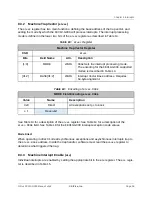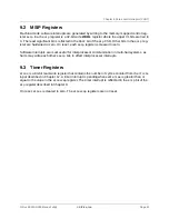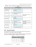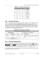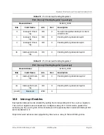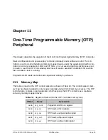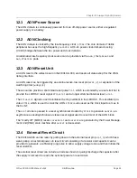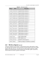
Offset
Name
Description
0x14
otp_mr
OTP device mode register
0x18
otp_mrr
OTP read-voltage regulator control
0x1C
otp_mpp
OTP write-voltage charge pump control
0x20
otp_vrren
OTP read-voltage enable
0x24
otp_vppen
OTP write-voltage enable
0x28
otp_a
OTP device address
0x2C
otp_d
OTP device data input
0x30
otp_q
OTP device data output
0x34
otp_rsctrl
OTP read sequencer control
11.2
Programmed-I/O lock register (
otp_lock
)
The
otp_lock
register supports synchronization between the read sequencer and the pro-
grammed-I/O interface. When the lock is clear, memory-mapped reads may proceed. When the
lock is set, memory-mapped reads do not access the OTP device, and instead return
0
immedi-
ately.
The
otp_lock
should be acquired before writing to any other control register. Software can
attempt to acquire the lock by storing
1
to
otp_lock
. If a memory-mapped read is in progress,
the lock will not be acquired, and will retain the value
0
. Software can check if the lock was suc-
cessfully acquired by loading
otp_lock
and checking that it has the value
1
.
After a programmed-I/O sequence, software should restore the previous value of any control
registers that were modified, then store
0
to
otp_lock
.
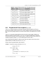
Listing 1 shows the synchronization code sequence.
Listing 1:
Sequence to acquire and release
otp_lock
.
la t0, otp_lock
li t1, 1
loop: sw t1, (t0)
lw t2, (t0)
beqz t2, loop
#
# Programmed I/O sequence goes here.
#
sw x0, (t0)
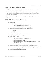
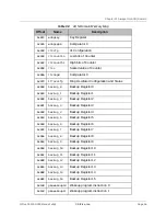
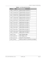
Table 29:
Register offsets within the OTP Controller memory map
Chapter 11 One-Time Programmable Memory (OTP)
SiFive FE310-G000 Manual: v3p2
© SiFive, Inc.
Page 50

