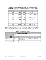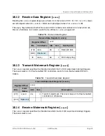
18.12
Receive Data Register (
rxdata
)
Reading the
rxdata
register dequeues a frame from the receive FIFO. For
fmt.len
< 8, values
are left-aligned when
fmt.endian
= MSB and right-aligned when
fmt.endian
= LSB.
The
empty
flag indicates whether the receive FIFO contains new entries to be read; when set,
the
data
field does not contain a valid frame. Writes to
rxdata
are ignored.
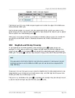
Receive Data Register (
rxdata
)
Register Offset
0x4C
Bits
Field Name
Attr.
Rst.
Description
[7:0]
data
RO
X
Received data
[30:8]
Reserved
31
empty
RW
X
FIFO empty flag
18.13
Transmit Watermark Register (
txmark
)
The
txmark
register specifies the threshold at which the Tx FIFO watermark interrupt triggers.
The reset value is
1
for flash-enabled SPI controllers, and
0
for non-flash-enabled SPI con-
trollers.
Transmit Watermark Register (
txmark
)
Register Offset
0x50
Bits
Field
Name
Attr.
Rst.
Description
[2:0]
txmark
RW
X
Transmit watermark. The reset value is 1 for flash-enabled
controllers, 0 otherwise.
[31:3]
Reserved
18.14
Receive Watermark Register (
rxmark
)
The
rxmark
register specifies the threshold at which the Rx FIFO watermark interrupt triggers.
The reset value is
0x0
.
Table 75:
Receive Data Register
Table 76:
Transmit Watermark Register
Chapter 18 Serial Peripheral Interface (SPI)
SiFive FE310-G000 Manual: v3p2
© SiFive, Inc.
Page 90

