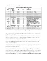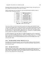
Breakpoint Control Register (
mcontrol
)
Register Offset
CSR
Bits
Field
Name
Attr.
Rst.
Description
0
R
WARL
X
Address match on LOAD
1
W
WARL
X
Address match on STORE
2
X
WARL
X
Address match on Instruction FETCH
3
U
WARL
X
Address match on User Mode
4
S
WARL
X
Address match on Supervisor Mode
5
Reserved
WPRI
X
Reserved
6
M
WARL
X
Address match on Machine Mode
[10:7]
match
WARL
X
Breakpoint Address Match type
11
chain
WARL
0
Chain adjacent conditions.
[17:12]
action
WARL
0
Breakpoint action to take. 0 or 1.
18
timing
WARL
0
Timing of the breakpoint. Always 0.
19
select
WARL
0
Perform match on address or data.
Always 0.
20
Reserved
WPRI
X
Reserved
[26:21]
maskmax
RO
4
Largest supported NAPOT range
27
dmode
RW
0
Debug-Only access mode
[31:28]
type
RO
2
Address/Data match type, always 2
Table 105:
Test and Debug Data Register 3
The
type
field is a 4-bit read-only field holding the value 2 to indicate this is a breakpoint con-
taining address match logic.
The
bpaction
field is an 8-bit read-write
WARL
field that specifies the available actions when
the address match is successful. The value 0 generates a breakpoint exception. The value 1
enters debug mode. Other actions are not implemented.
The R/W/X bits are individual
WARL
fields, and if set, indicate an address match should only be
successful for loads/stores/instruction fetches, respectively, and all combinations of imple-
mented bits must be supported.
The M/S/U bits are individual
WARL
fields, and if set, indicate that an address match should
only be successful in the machine/supervisor/user modes, respectively, and all combinations of
implemented bits must be supported.
The
match
field is a 4-bit read-write
WARL
field that encodes the type of address range for
breakpoint address matching. Three different
match
settings are currently supported: exact,
NAPOT, and arbitrary range. A single breakpoint register supports both exact address matches
and matches with address ranges that are naturally aligned powers-of-two (NAPOT) in size.
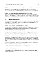
Breakpoint registers can be paired to specify arbitrary exact ranges, with the lower-numbered
breakpoint register giving the byte address at the bottom of the range and the higher-numbered
Copyright © 2019, SiFive Inc. All rights reserved.
107
Summary of Contents for FE310-G002
Page 1: ...SiFive FE310 G002 Manual v19p05 SiFive Inc ...
Page 11: ...Figure 1 FE310 G002 top level block diagram Copyright 2019 SiFive Inc All rights reserved 9 ...
Page 15: ...Chapter 2 List of Abbreviations and Terms 13 ...
Page 23: ...Chapter 4 Memory Map The memory map of the FE310 G002 is shown in Table 4 21 ...


