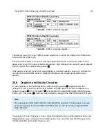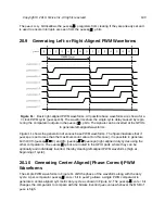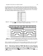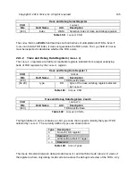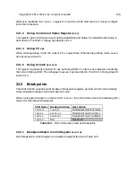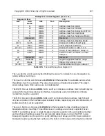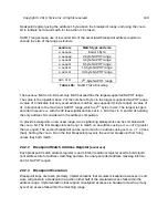
The JTAG DTM implements the BYPASS and IDCODE instructions.
On the FE310-G002, the IDCODE is set to
0x20000913
.
The JTAG DEBUG instruction gives access to the SiFive debug module by connecting the
debug scan register between
jtag_TDI
and
jtag_TDO
.
The debug scan register includes a 2-bit opcode field, a 7-bit debug module address field, and a
32-bit data field to allow various memory-mapped read/write operations to be specified with a
single scan of the debug scan register.
These are described in
The RISC‑V Debug Specification 0.13
.
Copyright © 2019, SiFive Inc. All rights reserved.
113
Summary of Contents for FE310-G002
Page 1: ...SiFive FE310 G002 Manual v19p05 SiFive Inc ...
Page 11: ...Figure 1 FE310 G002 top level block diagram Copyright 2019 SiFive Inc All rights reserved 9 ...
Page 15: ...Chapter 2 List of Abbreviations and Terms 13 ...
Page 23: ...Chapter 4 Memory Map The memory map of the FE310 G002 is shown in Table 4 21 ...

