The SPI interface is described in more detail in Chapter 19.
The pulse width modulation (PWM) peripheral can generate multiple types of waveforms on
GPIO output pins and can also be used to generate several forms of internal timer interrupt.
The PWM peripherals are described in Chapter 20.
The FE310-G002 has an I²C controller to communicate with external I²C devices, such as sen-
sors, ADCs, etc.
The I²C is described in detail in Chapter 21.
The FE310-G002 provides external debugger support over an industry-standard JTAG port,
including 8 hardware-programmable breakpoints per hart.
Debug support is described in detail in Chapter 22, and the debug interface is described in
Chapter 23.
Copyright © 2019, SiFive Inc. All rights reserved.
12
Summary of Contents for FE310-G002
Page 1: ...SiFive FE310 G002 Manual v19p05 SiFive Inc ...
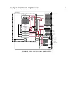
Page 11: ...Figure 1 FE310 G002 top level block diagram Copyright 2019 SiFive Inc All rights reserved 9 ...
Page 15: ...Chapter 2 List of Abbreviations and Terms 13 ...
Page 23: ...Chapter 4 Memory Map The memory map of the FE310 G002 is shown in Table 4 21 ...


