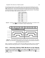
For flash-enabled SPI controllers, the reset value is
0x0008_0008
, corresponding to
proto
=
single,
dir
= Tx,
endian
= MSB, and
len
= 8. For non-flash-enabled SPI controllers, the reset
value is
0x0008_0000
, corresponding to
proto
= single,
dir
= Rx,
endian
= MSB, and
len
= 8.
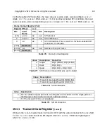
Frame Format Register (
fmt
)
Register Offset
0x40
Bits
Field
Name
Attr.
Rst.
Description
[1:0]
proto
RW
0x0
SPI protocol
2
endian
RW
0x0
SPI endianness
3
dir
RW
X
SPI I/O direction. This is reset to 1 for flash-enabled SPI
controllers, 0 otherwise.
[15:4]
Reserved
[19:16]
len
RW
0x8
Number of bits per frame
[31:20]
Reserved
Value
Description
Data Pins
0
Single
DQ0 (MOSI), DQ1 (MISO)
1
Dual
DQ0, DQ1
2
Quad
DQ0, DQ1, DQ2, DQ3
Value
Description
0
Transmit most-significant bit (MSB) first
1
Transmit least-significant bit (LSB) first
Value
Description
0
Rx: For dual and quad protocols, the DQ pins are tri-stated. For the single protocol,
the DQ0 pin is driven with the transmit data as normal.
1
Tx: The receive FIFO is not populated.
Writing to the
txdata
register loads the transmit FIFO with the value contained in the
data
field.
For
fmt.len
< 8, values should be left-aligned when
fmt.endian
= MSB and right-aligned
when
fmt.endian
= LSB.
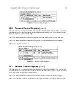
Table 76:
Frame Format Register
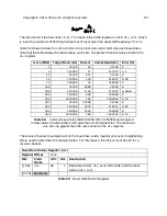
Table 77:
SPI Protocol. Unused DQ pins are tri-stated.
Table 78:
SPI Endianness
Table 79:
SPI I/O Direction
Copyright © 2019, SiFive Inc. All rights reserved.
90
Summary of Contents for FE310-G002
Page 1: ...SiFive FE310 G002 Manual v19p05 SiFive Inc ...
Page 11: ...Figure 1 FE310 G002 top level block diagram Copyright 2019 SiFive Inc All rights reserved 9 ...
Page 15: ...Chapter 2 List of Abbreviations and Terms 13 ...
Page 23: ...Chapter 4 Memory Map The memory map of the FE310 G002 is shown in Table 4 21 ...


