68
SDS2000X HD Service Manual
8.5.3 Check the clock
There are 3 clock oscillators and associated fanout buffers on board to source different circuits. Each
of them serves one or more functions. The voltage compliance of all the clocks under test is
LVCMOS33 or LVCMOS25.
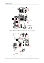
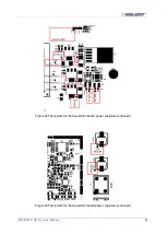
Table 19 Clock parameters of the Acquisition System
Clock
Frequency
Test Point
Compliance
Served Function
10.0000 MHz
± 2 ppm
TP103
LVCMOS33
10 MHz TCXO Output
TP104
LVCMOS33
Reference Clock for the Acquisition Clock
Generator
R772
LVCMOS33
Lock detection for the clock generator, NOT a
clock. Active high.
TP105
LVCMOS25
Reference Clock for the ACQ FPGA
33.3333 MHz
± 25 ppm
TP95
LVCMOS33
Reference Clock for the SMP CPU subsystem
24.0000 MHz
± 25 ppm
TP96
LVCMOS33
Reference Clock for the USB Controller 0
TP97
LVCMOS33
Reference Clock for the USB Controller 1
TP98
LVCMOS25
Reference Clock for USB Hub
TP99
LVCMOS25
Asynchronous Clock for the ACQ FPGA
25.0000 MHz
± 25 ppm
TP100
LVCMOS33
Reference Clock for the Ethernet Controller
TP101
LVCMOS33
Reference Clock for the CPLD
TP102
LVCMOS25
Reference Clock for the SMP FPGA subsystem
TP13
LVCMOS25
Reference Clock to the MMB FPGA

