SDS2000 X HD Ser vice Manual
71
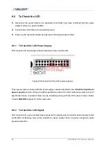
Figure 27 Test points for LCD signal
Table 20 Signal parameters of the LCD
Test Point
Signal
Compliance
Description
J8 PIN7
LCD ON
LVCMOS33
PWM signal to control the
brightness of the LCD.
Normally HIGH.
J8 PIN8/10
Data 0
LVDS
LCD DATA signal.
Always active.
J8 PIN11/13
Data 1
LVDS
LCD DATA signal.
Always active
J8 PIN16/18
Data 2
LVDS
LCD DATA signal.
Always active
J8 PIN19/21
Clock
LVDS
LCD reference clock.
If the signal is active, replace the LCD panel.
If the signal is stuck, double-check with the LCD cable disconnected. If the signal is still stuck,
replace the acquisition board. If not, replace the LCD panel or the LCDI board.

