background image

SC5312A Operating & Programming Manual 

Rev 1.0.2 


S C 5 3 1 2 A


T

H E O R Y   O F  

O

P E R A T I O N


Overview  

The  SC5312A  is  a  single-stage,  direct  conversion  Inphase-Quadrature  (IQ)  demodulating  mixer.  The 
SC5312A  can  operate  as  a  single-stage  downconverter  or  as  an  IQ  demodulator.  The  SC5312A 
demodulator operates in the 400 MHz to 6 GHz RF range with a typical 3 dB IF bandwidth of 160 MHz in 
single-stage converter mode, or 320 MHz in IQ mode. The RF input stage has adjustable gain to allow the 
user to adjust the incoming RF signal prior to the demodulation process for the purpose of optimizing RF 
dynamic range. The IF stage has adjustable gain to ensure that linearity and noise of the IF output are 
optimized. The SC5312A has the necessary RF amplifiers, attenuators, IF amplifiers, and IF control via DACs 
to allow the user to optimally operate the device over the entire frequency range as well as for both small 
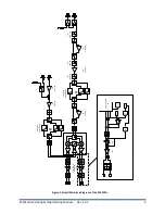
and large RF input levels. Figure 2 shows a simplified block diagram of the SC5312A, showing only the 
signal conditioning components critical for the following discussion. The following sections provide an in-
depth discussion on how to optimize the converter for linearity and signal-to-noise dynamic range.  

RF Input Section  

In  the  design  of  the  RF  input  section,  care  was  taken  to  ensure  that  the  dynamic  range  of  the  IQ 
demodulator is preserved as seen at the input port of the device. This requires that the demodulator is 
not driven too hard (high signal amplitude) or too soft (low signal amplitude). When the device is driven 
hard,  nonlinear  effects  dominate  the  system.  When  driven  too  softly,  signal-to-noise  dynamic  range 
suffers. A general rule is to apply more attenuation earlier in the RF signal path to improve linearity, and 
more gain to improve signal-to-noise performance. As an example, for a given input signal level and while 
maintaining a relatively constant output IF level, the user would switch in RF AMP#1 and apply attenuation 
on ATTEN#3 to improve signal-to-noise dynamic range. The factory default state sets all the RF amplifiers 
off, all attenuators to 0 dB attenuation, and the IF gain to 8 dB (DAC code of 32). In this default state, the 
device is optimized for a -10 dBm RF signal in the 1.0 GHz to 2.4 GHz range. The IF output is typically 0.5 
V - 1.0 V peak-to-peak differential at these settings.    

The RF amplifiers are used to improve the gain of the device if the input signal is too low or when the 
losses at higher frequencies are large. RF AMP#1 is usually selected when the RF signals are lower than -
25 dBm at the input port. With RF AMP#1 enabled, the device sensitivity is improved and the detection of 
low level signals is better resolved. RF AMP#2 should be selected and switched into the signal path at RF 
frequencies  greater  than  5  GHz,  where  the  signal  power  loss  through  the  front  end  prior  to  the 
demodulator can be as high as 15 dB due to filter and switch insertion losses. At these high RF frequencies, 
if the IF gain is at its maximum of 15.75 dB (DAC code = 63) and the IF output level falls below -10 dBm (or 
outside the digitizers optimal levels), RF AMP#2 should be enabled.  

Summary of Contents for SC5312A

Page 1: ...SC5312A 400 MHz to 6 GHz IQ Demodulator PXI Express Interface Operating and Programming Manual 2013 2020 SignalCore Inc support signalcore com...

Page 2: ...guring the SC5312A 4 RF Signal Connections 6 Baseband Connections 7 Indicator LED 7 SC5312A Theory of Operation 8 Overview 8 RF Input Section 8 LO Input Section 10 IF Output Section 11 SC5312A Program...

Page 3: ...put Linearity of the IQ Demodulator 15 Storing the Startup State 15 Writing to the User EEPROM 16 Querying the SC5312A Writing to Request Registers 17 Reading the Device Temperature 17 Reading the Dev...

Page 4: ...RT OF SIGNALCORE INCORPORATED SHALL BE LIMITED TO THE AMOUNT THERETOFORE PAID BY THE CUSTOMER SIGNALCORE INCORPORATED WILL NOT BE LIABLE FOR DAMAGES RESULTING FROM LOSS OF DATA PROFITS USE OF PRODUCTS...

Page 5: ...materials and the categorical amount present in our products are shown below Model Name Lead Pb Mercury Hg Cadmium Cd Hexavalent Chromium Cr VI Polybrominated biphenyls PBB Polybrominated diphenyl eth...

Page 6: ...SOFTWARE UNANTICIPATED USES OR MISUSES OR ERRORS ON THE PART OF THE USER OR APPLICATIONS DESIGNER ADVERSE FACTORS SUCH AS THESE ARE HEREAFTER COLLECTIVELY TERMED SYSTEM FAILURES ANY APPLICATION WHERE...

Page 7: ...e specifications The SC5312A is designed to be sufficiently cooled in either all PXIe chassis or PXIe hybrid chassis PXI Express chassis with traditional PXI slots However certain environmental factor...

Page 8: ...v 1 0 2 5 The SC5312A is a PXIe based IQ demodulator with all I O connections and indicators located on the front face of the module as shown below Each location is discussed in further detail below F...

Page 9: ...trapped inside the connector may take several days to fully evaporate and may degrade measurement performance until fully evaporated Tighten all SMA connections to 5 in lb max 56 N cm max RF Signal C...

Page 10: ...ration it is recommended to terminate the other half of the differential pair using a 50 terminator All baseband connectors are MCX female Indicator LED The SC5312A provides visual indication of impor...

Page 11: ...d high signal amplitude or too soft low signal amplitude When the device is driven hard nonlinear effects dominate the system When driven too softly signal to noise dynamic range suffers A general rul...

Page 12: ...ocm Variable Diff Amp Vocm Vocm Out Diff Amp IQ Demodulator Linearity Dac 90 0 i i 50W 50W RF Amp 1 RF Amp 3 RF Amp 2 9 Selectable RF Filters 9 Selectable LO Filters LO Amp 2 LO Amp 1 Gain Selectable...

Page 13: ...situ equalization to remove IQ errors such as phase imbalance and quadrature gain offsets that are inherent to the device Providing this auxiliary path makes the task of characterizing the system with...

Page 14: ...of the device This is not a hard requirement and the user will need to adjust the voltage levels to suit their specific requirements As an example setting to some other voltage may be required to opt...

Page 15: ...t computer should identify the device and load the appropriate driver For more information please see the SC5312A_Readme txt file also located under the Win directory A LabVIEW API is provided and it...

Page 16: ...Bit 6 Bit 5 Bit 4 Bit 3 Bit 2 Bit 1 Bit 0 INITIALIZE 0x01 7 0 Mode SET_SYSTEM_ACTIVE 0x02 7 0 Enable SYS LED RF_FREQUENCY 0x10 7 0 MHz Frequency Word 7 0 15 8 MHz Frequency Word 15 8 23 16 MHz Frequen...

Page 17: ...ta is sent as a 40 bit word with the LSB in Hz Setting RF Input RF Amplifiers RF_AMPLIFIER 0x12 This register enables or disables the RF amplifiers Setting bit 0 low 0 disables the RF amplifier Settin...

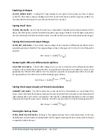
Page 18: ...Offset in Differential Amplifiers DC_OFFSET_DAC 0x1A The DC offset between the and terminals of the differential amplifier output can be minimized by writing this DAC Varying the DAC value from 0 to 1...

Page 19: ...EEPROM for the user to store data User data is sent one byte at a time and is contained in the last least significant byte of the three bytes of data written to the register The other two bytes contai...

Page 20: ...st 14 bits 13 0 Bit 13 is the polarity bit indicating whether it is positive 0x0 or negative 0x1 For an ENDPOINT_IN transfer data is returned in 2 bytes with the MSB first The temperature value repres...

Page 21: ...0x8000 will return data stored in address location 0x0000 The calibration EEPROM map is shown in Table 5 All calibration data whether floats unsigned 8 bit unsigned 16 bit or unsigned 32 bit integers...

Page 22: ...M map EEPROM ADDRESS HEX NUMBER OF DATA POINTS TYPE DESCRIPTION 0 1 U32 Manufacturing Information 4 1 U32 Product serial number 8 1 U32 RF module number C 1 U32 Product manufacture date 24 1 F32 Firmw...

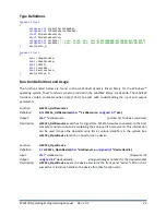
Page 23: ...ce sc5312a_SetFrequency sc5312a_SetRfGain sc5312a_SetRfAmplifier sc5312a_SetRfPath sc5312a_SetLoOut sc5312a_SetRfAttenuation sc5312a_SetRfFilter sc5312a_SetLoFilter sc5312a_SetIfGainDac sc5312a_SetVco...

Page 24: ...set the device active LED define RF_FREQUENCY 0x10 set the frequency define RF_AMPLIFIER 0x12 enable amplifiers define RF_ATTENUATION 0x13 set attenuation for digital step attenuators define RF_PATH...

Page 25: ...rl H to assist with understanding the input and output parameters Function sc5312a_ListResources Definition int sc5312a_ListResources char visaResource unsigned int size Output char visaResource point...

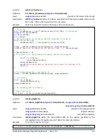
Page 26: ...r specified by the commandByte See the register map on Table 2 for more information Example To set the frequency to 2 GHz Declaring char visaResource char malloc sizeof char 10 10 devices unsigned int...

Page 27: ...l mode set the mode of initialization Description sc5312a_InitDevice initializes resets the device Mode 0 resets the device to the default power up state Mode 1 resets the device but leaves it in its...

Page 28: ...char attenuator unsigned char atten Input unsigned int deviceHandle handle to the opened device unsigned char attenuator selects the attenuator to program unsigned char atten attenuation value 0 31 d...

Page 29: ...the differential amplifiers The default factory setting is 2008 Function sc5312a_SetDcOffsetDac Definition int sc5312a_SetDcOffsetDac unsigned int deviceHandle unsigned char channel unsigned short dac...

Page 30: ...sc5312a_GetDeviceInfo unsigned int deviceHandle deviceInfo_t devInfo Input unsigned int deviceHandle handle to the opened device Output deviceInfo_t devInfo device info struct Description sc5312a_Get...

Page 31: ...gned char byteData Input unsigned int deviceHandle handle to the opened device unsigned int memAdd EEPROM memory address Output unsigned char byteData the read back byte data Description sc5312a_ReadU...

Page 32: ...receive a factory calibration The SC5312A is sold as a component and users will need to perform amplitude and IQ correction as part of their system which may minimally include a digitizer LO source an...

Reviews: