background image

GreenPAK Universal 

Development Board


Silego Technology Inc.      

www.silego.com


10/13/2014                              


3.2. Functional Description 

3.2.1. Power Supply 


Main  power  source  of  GreenPAK3  Universal  Board  is  USB  power  lines.  GreenPAK3 

chip power supply range is 1.8-5.5 volts. The development board can provide power from 0 to 
5.5V. To provide this power range the development board is enabled with a boost converter. A 
Signal  generator  with  a  buffered  output  controls  GreenPAK3  chip  power  rail.  For  more 
information about GreenPAK3 electrical specification, please refer to the part datasheet. 
 

3.2.2. USB Communication 


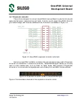
The board has a USB communications interface that uses the USB mini-B connector, as 

shown  in  Figure  3-2.  This  interface  provides  communication  with  software  control  tool  and 
supplies power to the board, as discussed in 

Power Supply chapter. 


Figure 3-2. USB Interface 

3.2.3. GND connections 


There are 6 GND pins on the left side, 6 pins and 1 header on the right side. These can 

be  used  for  test  equipment  (oscilloscope,  multimeter  etc.)  ground  reference  connection  or  to 
connect external test circuitry ground. 

3.2.4. Pin test points 


Each GreenPAK3 chip pin including VDD has its own observation test point. These test 

points  were  designed  only  for  observation,  if  you  need  to  connect  an  external  signal  source, 
use a software-controlled expansion connector.  

3.2.5. LEDs  


All the pins except Pin2 can be connected to buffered LEDs. This option allows you to 

visualize digital levels on chip pins. There are 2 selection modes:  

-  Buffered LED (with high impedance input); 

Summary of Contents for GreenPAK

Page 1: ...GreenPAK Universal Development Board User Guide Silego Technology Corporate Headquarters 1715 Wyatt Drive Santa Clara CA 95054 USA Phone 408 327 8800 http www silego com ...

Page 2: ...and foreign United States copyright laws and international treaty provisions Silego hereby grants to licensee a personal non exclusive non transferable license to copy use modify create derivative works of and compile the Silego Source Code and derivative works for the sole purpose of creating custom software and or firmware in support of licensee product to be used only in conjunction with a Sile...

Page 3: ... Install Software 6 2 4 Uninstall Software 6 3 Hardware 7 3 1 Overview 7 3 2 Functional Description 8 3 2 1 Power Supply 8 3 2 2 USB Communication 8 3 2 3 GND connections 8 3 2 4 Pin test points 8 3 2 5 LEDs 8 3 2 6 Socket connector 9 3 2 7 Expansion connector 10 3 2 8 Pins connectivity 15 4 Example projects 18 4 1 Project Counter with clock enable 18 4 2 Project LED string with direction 31 A App...

Page 4: ...ner GreenPAK3 Designer is an easy to use full featured integrated development environment IDE that allows you to specify exactly how you want the device to be configured This provides you a direct access to all GreenPAK3 device features and complete control over the routing and configuration options GreenPAK3 Designer has simple and intuitive software interface to GreenPAK3 Universal Board that gi...

Page 5: ...e online at http www silego com At silegousa silegochinese silegoeurope silegojapan At Silego Technology GreenPAK3 Designer will update itself when a new software version is detected and available For manual updates please go to Software Docs page at Silego Technology website You can also find all these resources in the Help menu of GreenPAK3 Designer ...

Page 6: ...on provides the schematics and BOM associated with the GreenPAK3 Universal Board 2 2 Install Hardware No hardware installation is required for this kit 2 3 Install Software GreenPAK3 Designer software is available free of charge from the Silego website at Software Docs page 2 4 Uninstall Software The software can be uninstalled in the way typical for your operating system Please refer to your oper...

Page 7: ...3 1 Overview Figure 3 1 GreenPAK3 Universal Board top view Notification All test points were designed only for observation of signals on the pins Please do not try to connect external power signal source to test points this will affect GreenPAK3 Universal Board functionality and may even damage it ...

Page 8: ...or as shown in Figure 3 2 This interface provides communication with software control tool and supplies power to the board as discussed in Power Supply chapter Figure 3 2 USB Interface 3 2 3 GND connections There are 6 GND pins on the left side 6 pins and 1 header on the right side These can be used for test equipment oscilloscope multimeter etc ground reference connection or to connect external t...

Page 9: ...3 2 6 Socket connector The GreenPAK3 Universal Board is supplied with a detachable socket board Figure 3 3 Its main purpose is to connect GreenPAK3 chip to the Development Board It can be used to have an easy way to use programmed chip in external circuits or measure current consumption of your project Figure 3 3 GreenPAK3 Socket Board and schematic Figure 3 4 GreenPAK3 Socket PCB ...

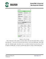
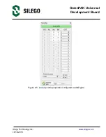
Page 10: ...vailable on Figure 3 5 Figure 3 5 GreenPAK3 expansion connector schematic Each pin except PIN11 GND is controlled through individual analog switch Expansion connector is a standard 0 1 double row connector GreenPAK3 Designer allows you to easily open or close external pins as it is shown on figure below Main purpose of Expansion connector is to connect external signal power source safety for Green...

Page 11: ...hip is required inside the socket When the Test mode button is pressed the software will first read the chip to verify that it was inserted and then configure the GreenPAK3 Universal Board as it was set in Emulation Tool window When the Test mode button is grey then the Dev Board is in Default state and all expansion port switches are open disconnected After Emulation button is pressed the softwar...

Page 12: ...socket can also be used for the in circuit development with programmed chips the board and socket connectors have same pinout The GreenPAK Universal Board provides three possible ways of using expansion connector 1 The internal power is used to run chip no external power output is needed external signal sources and loads can be connected between pins and GND The configuration steps close internal ...

Page 13: ...eenPAK chip is already programmed user can use Emulation mode to load some other project and test it on the emulation tool during the Emulation mode in that case emulation data will be cleared The Emulation mode is not necessary for checking programmed parts in this case the Test mode is enough Expansion connector can be divided on 3 types of connections 1 VDD 2 GND 3 Data connections VDD connecti...

Page 14: ...GreenPAK Universal Development Board Silego Technology Inc www silego com 10 13 2014 Figure 3 10 Expansion connector Pin with protection resistor ...

Page 15: ...of loads and signal sources Each source has its own special purpose List of available connections for each pin is presented in the table below Pin Set to VDD Set to GND Pull up Pull down Set configurable button LED Signal generator Logic generator 1 2 3 4 5 6 7 8 VDD Pin2 Pin3 Pin4 Pin5 Pin6 Pin7 Pin8 Pin9 Pin10 Pin12 Pin13 Pin14 Pin15 Pin16 Pin17 Pin18 Pin19 Pin20 ...

Page 16: ...ading schematics Set to VDD Set to VDD Set to GND Set to GND Pull up Pull up Pull down Pull down Button pressed Button pressed Button released Button released Button with different configurations Button VDD HI Z Button HI Z GND Button VDD GND Button Pull up Pull down Button Pull up GND Button VDD Pull down ...

Page 17: ...Inc www silego com 10 13 2014 LED Buffered LED LED Inverted buffered LED VDD Signal generator VDD Signal generator VDD Signal generator works similar to other Signal generators but has wider output voltage range It can provide maximum supply level of 5 5 V ...

Page 18: ...om 10 13 2014 4 Example projects 4 1 Project Counter with clock enable The first example project Counter with clock enable is very simple For this project we will need 2 digital inputs 1 digital output 1 Look Up table with two inputs 1 Counter Figure 4 1 GreenPAK3 Designer ...

Page 19: ...GreenPAK Universal Development Board Silego Technology Inc www silego com 10 13 2014 Figure 4 2 GreenPAK3 Components list ...

Page 20: ...in Pin Name Type Pin Description 1 VDD PWR Supply Voltage 2 Clock Digital input Digital Input 3 Enable Digital input Digital Input 11 GND GND Ground 20 Counter Output Push pull output Digital Output On Figure 4 1 there are shown all the components used in project next step is to configure selected blocks Double click on PIN20 to open Properties panel Select 1x push pull from the drop down menu in ...

Page 21: ...this design is Look Up table First Look Up LUT4 table is used to generate logic 1 only when there are high logic levels on both inputs AND gate Select AND gate from Standard gates drop down menu or set table manually Second Look Up LUT5 configured as NOR gate It is used to generate reset signal for counter on PIN3 falling edge ...

Page 22: ...GreenPAK Universal Development Board Silego Technology Inc www silego com 10 13 2014 Figure 4 4 Look Up table properties configured as AND gate ...

Page 23: ...GreenPAK Universal Development Board Silego Technology Inc www silego com 10 13 2014 Figure 4 5 Look Up table properties configured as AND gate ...

Page 24: ...014 Figure 4 4 Counter properties Final step is to connect used components Use Wire tool to perform this action To connect two pins select Set Wire and then click on the first and the second pin of the module or modules that you want to connect The trace will be automatically routed ...

Page 25: ...igner Figure 4 5 displays ready project with configured blocks and wire connections Use the GreenPAK Universal Board to test this project Connect GreenPAK Universal Board to PC and press Emulation button This will load code of your project to the chip and will enable Test Board functionality of your Dev Board ...

Page 26: ...rator is applied on VDD pin to power GreenPAK3 chip Logic generator Logic generator serves as clock source Button is a software simulation of the real button It switches PIN between VDD and GND signal levels Inverted buffered LED Buffered LED Figure 4 7 Signal generator connected to VDD pin Signal generator is presented as power source for GreenPAK3 chip It s configured to output source constant 3...

Page 27: ...pment Board Silego Technology Inc www silego com 10 13 2014 Figure 4 8 Signal generator settings Logic generator s purpose is to provide counter module clock pulses It is configured as 10 Hz clock source as shown on Figure 4 9 ...

Page 28: ...GreenPAK Universal Development Board Silego Technology Inc www silego com 10 13 2014 Figure 4 9 Logic generator properties ...

Page 29: ...enta 3rd line Counter output Figure 4 11 Waveform triggered on button pressed Channel 1 yellow top Logic generator Channel 2 light blue 2nd line Button 1 enable Counter 0 disable Counter Channel 3 magenta 3rd line Counter output Figure 4 12 Waveform no trigger and button released Channel 1 yellow top Logic generator Channel 2 light blue 2nd line Button 1 enable Counter 0 disable Counter Channel 3 ...

Page 30: ...pment Board Silego Technology Inc www silego com 10 13 2014 Figure 4 13 Waveform impulse width of Logic generator and count end signal As it is shown on Figure 4 12 and Figure 4 13 Counter works only when the button is pressed ...

Page 31: ...com 10 13 2014 4 2 Project LED string with direction For this project we will need Analog pin for input data Digital pin for PWM output ADC block PWM block Figure 4 14 Used blocks for current project For testing this project we will use Signal generator with sine waveform ...

Page 32: ...GreenPAK Universal Development Board Silego Technology Inc www silego com 10 13 2014 Figure 4 15 Sine waveform generated with ...

Page 33: ...GreenPAK Universal Development Board Silego Technology Inc www silego com 10 13 2014 Figure 4 16 Emulation window with Buffered LED and Signal generator ...

Page 34: ...lego com 10 13 2014 Pin Configuration Pin Pin Name Type Pin Description 1 VDD PWR Supply Voltage 2 DIRECTION Input Controls direction 6 SIGNAL Input Analog Input 11 GND GND Ground 15 LED_A Output LED 17 LED_B Output LED 19 LED_C Output LED Figure 4 17 Pin properties ...

Page 35: ...eenPAK Universal Development Board Silego Technology Inc www silego com 10 13 2014 Pin 6 is configured as analog input output This pin will be used for generating SINE waveform Figure 4 18 Pin properties ...

Page 36: ...GreenPAK Universal Development Board Silego Technology Inc www silego com 10 13 2014 Figure 4 19 ACMP properties Pin 15 17 19 output pins with 1x push pull They are an observing pin ...

Page 37: ...e comparator will set logic 1 on its output In this project 3 comparators are used ACMP0 positive input is 200mV ACMP1 is 500mV and ACMP2 is 800mV In this case we will have 4 states all LEDs are off LED_A is on LED_A and LED_B are on All LEDs are on If Pin 2 logic level will be set to 1 this states will transform into all LEDs are on LED_A and LED_B are on LED_A is on All LEDs are off Figure 4 21 ...

Page 38: ...4 Functionality Waveform Channel 1 yellow top Direction Channel 2 light blue 2nd line LED_A Channel 3 magenta 3rd line LED_B Channel 4 blue 4rth line LED_C Figure 4 22 Direct direction Figure 4 23 Opposite direction The PWM duty cycle rises up to 100 when analog signal is close to 1V ...

Page 39: ...GreenPAK Universal Development Board Silego Technology Inc www silego com 10 13 2014 A Appendix A 1 Schematic MCU ...

Page 40: ...GreenPAK Universal Development Board Silego Technology Inc www silego com 10 13 2014 Analog switches protection diodes and LEDs ...

Page 41: ...GreenPAK Universal Development Board Silego Technology Inc www silego com 10 13 2014 Socket and expansion connectors Signal generators ...

Page 42: ...GreenPAK Universal Development Board Silego Technology Inc www silego com 10 13 2014 Boost converter USB interface Port extender ...

Page 43: ...GreenPAK Universal Development Board Silego Technology Inc www silego com 10 13 2014 USB protection ...

Page 44: ...8 7 BAS21SLT1G SOT 23 3 19 D7 D25 8 GM1JS35200AE 0603 1608 Metric 1 LED1 9 LB Q39E N1P1 35 1 0603 1608 Metric 1 LED2 10 LW Q38G Q1S1 3K6L 1 0603 1608 Metric 1 LED3 11 LTST C193KGKT 5A 0603 1608 Metric 17 LED4 LED20 12 NX5032GA 25 0MHZ LN CD 1 2 SMD 1 X1 13 SC4503TSKTRT TSOT23 5 1 IC3 14 USB M26FTR 1 CONN1 15 2N7002 SOT 23 3 2 Q1 Q2 16 MBRX120 TP SOD 123 4 D3 D6 17 SLG59M610V TDFN 8 1 IC4 18 AD8591...

Page 45: ... 28 GRM155F51C104ZA01D 0402 1005 metric 28 C6 C13 C16 C19 C20 C22 C23 C27 C28 C30 C31 C33 C35 C36 C37 C38 C40 C41 C42 C44 C46 C47 C48 C49 C50 C51 C54 Csoc 29 EMK316BJ106KL T 1206 3216 metric 7 C2 C3 C4 C7 C14 C26 C32 30 C2012X7R1C105K 1 25 0805 2012 metric 4 C21 C29 C45 C39 31 CC0402KRX7R9BB103 0402 1005 Metric 4 C5 C15 C52 C55 33 CC0402JRNPO9BN220 0402 1005 metric 8 C1 C17 C18 C24 C25 C34 C43 C53...

Page 46: ...6W 1 0402 1005 metric 1 R5 41 RESISTOR 2k 1 16W 0402 1005 metric 6 R22 R23 R24 R33 R34 R2 42 RESISTOR 24 ohm 1 16W 0402 1005 metric 2 R14 R17 43 RESISTOR 2 ohm 0805 2012 metric 1 R29 44 YC164 JR 072KL 1206 3216 metric 4 RN6 RN7 RN8 RN9 45 YC164 JR 07100RL 1206 3216 metric 5 RN1 RN2 RN3 RN4 RN5 54 RESISTOR 0 ohm 1206 3216 metric 1 R35 55 SLG55321 TDFN 8 1 IC1 56 BZV55C5V6 TP SOD 80C 1 D1 46 5000_ 1...

Page 47: ...GreenPAK Universal Development Board Silego Technology Inc www silego com 10 13 2014 51 SSQ 110 02 T D RA 0 100 2 54mm 1 SV1 52 961106 6404 AR 0 100 2 54mm 2 SV2 SV3 53 3021009 06 1 ...

Page 48: ...Mouser Electronics Authorized Distributor Click to View Pricing Inventory Delivery Lifecycle Information Silego SLG4DVK5 SLG4DVK4 SLG4DVKDS SLG4DVK1 SLG4DVKADV ...

Reviews: