


S i 5 3 x x - R M
106
Rev. 0.52
8.2. Output Clock Drivers
The output clocks can be configured to be compatible with LVPECL, CML, LVDS, or CMOS as shown in Table 56.
Unused outputs can be left unconnected. For microprocessor-controlled devices, it is recommended to write
“disable” to
SFOUTn
to disable the output buffer and reduce power. When the output mode is CMOS, bypass
mode is not supported.
8.2.1. LVPECL TQFP Output Signal Format Restrictions at 3.3 V (Si5367, Si5368, Si5369)
The LVPECL and CMOS output formats draw more current than either LVDS or CML; however, there are
restrictions in the allowed output format pin settings so that the maximum power dissipation for the TQFP devices
is limited when they are operated at 3.3 V. When Vdd = 3.3 V and there are four enabled LVPECL or CMOS
outputs, the fifth output must be disabled. When Vdd = 3.3 V and there are five enabled outputs, there can be no
more than three outputs that are either LVPECL or CMOS. All other configurations are valid, including those with
Vdd = 2.5 V.
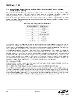
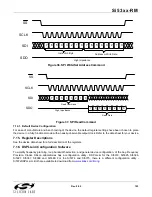
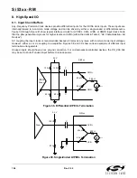
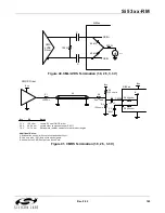
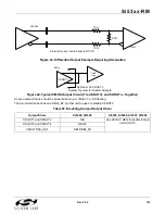
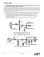
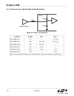
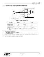
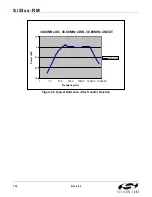
8.2.2. Typical Output Circuits
It is recommended that the outputs be ac coupled to avoid common mode issues. This suggestion does not apply
to the Si5366 and Si5368 when CKOUT5 is configured as FS_OUT (frame sync) because it can a have a duty
cycle significantly different from 50%.
Figure 42. Typical Output Circuit (Differential)
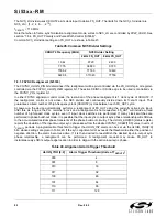
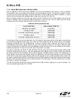
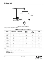
Table 56. Output Driver Configuration
Output Mode
SFOUTn Pin Settings
(Si5316, Si5322, Si5323, Si5365)
SFOUTn_REG [2:0] Settings
(Si5319, Si5325, SI5326, Si5327,
Si5367, Si5368, Si5369, Si5374,
Si5375)
LVDS
HM
111
CML
HL
110
LVPECL
MH
101
Low-swing
LVDS
ML
011
CMOS
LH
010
Disabled
LM
000
Reserved
All Others
All Others
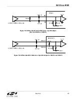
Note:
The LVPECL outputs are “LVPECL compatible.” No DC biasing circuitry is required to drive a
standard LVPECL load.
Si53xx
Rcvr
100
Z0 = 50
Z0 = 50
Summary of Contents for Si5316 Series
Page 2: ...Si53xx RM 2 Rev 0 52 ...
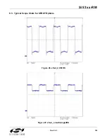
Page 110: ...Si53xx RM 110 Rev 0 52 Figure 48 sfout_5 LVPECL Figure 49 sfout_6 CML ...
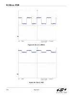
Page 111: ...Si53xx RM Rev 0 52 111 Figure 50 sfout_7 LVDS ...
Page 127: ...Si53xx RM Rev 0 52 127 Figure 66 155 52 MHz In 622 08 MHz Out Loop BW 7 Hz Si5324 ...
Page 128: ...Si53xx RM 128 Rev 0 52 Figure 67 19 44 MHz In 156 25 MHz Out Loop BW 80 Hz ...
Page 129: ...Si53xx RM Rev 0 52 129 Figure 68 19 44 MHz In 156 25 MHz Out Loop BW 5 Hz Si5324 ...
Page 131: ...Si53xx RM Rev 0 52 131 Figure 70 61 44 MHz In 491 52 MHz Out Loop BW 7 Hz Si5324 ...
Page 132: ...Si53xx RM 132 Rev 0 52 Figure 71 622 08 MHz In 672 16 MHz Out Loop BW 6 9 kHz ...
Page 133: ...Si53xx RM Rev 0 52 133 Figure 72 622 08 MHz In 672 16 MHz Out Loop BW 100 Hz ...
Page 134: ...Si53xx RM 134 Rev 0 52 Figure 73 156 25 MHz In 155 52 MHz Out ...
Page 139: ...Si53xx RM Rev 0 52 139 Figure 78 86 685 MHz In 173 371 MHz Out ...
Page 140: ...Si53xx RM 140 Rev 0 52 Figure 79 86 685 MHz In 693 493 MHz Out ...
Page 142: ...Si53xx RM 142 Rev 0 52 Figure 81 10 MHz In 1 GHz Out ...
Page 174: ...Si53xx RM 174 Rev 0 52 Figure 99 Si5374 Si5375 DSPLL A ...
Page 175: ...Si53xx RM Rev 0 52 175 Figure 100 Si5374 Si5375 DSPLL B ...
Page 176: ...Si53xx RM 176 Rev 0 52 Figure 101 Si5374 Si5375 DSPLL C ...