


S i 5 3 x x - R M
108
Rev. 0.52
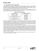
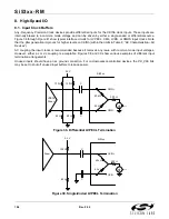
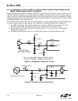
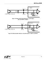
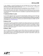
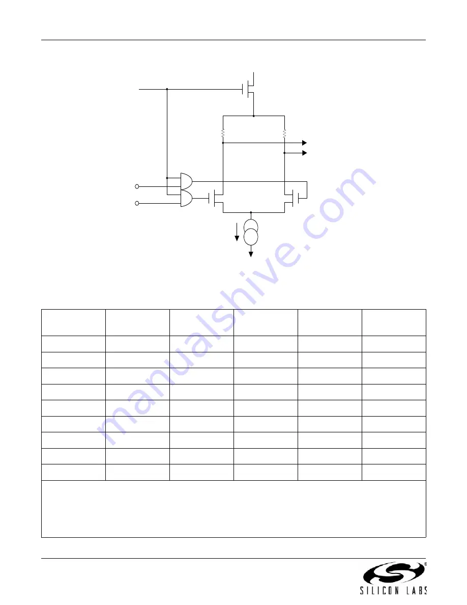
Figure 45. CKOUT Structure
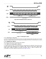
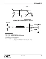
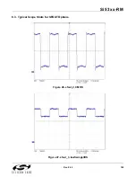
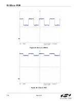
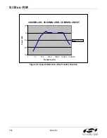
8.2.3. Typical Clock Output Scope Shots
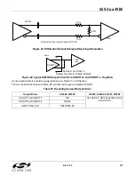
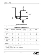
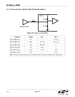
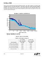
Table 58. Output Format Measurements
1,2
Name
SFOUT Pin
SFOUT Code
Single
Vpk–pk
Diff
Vpk–pk
Vocm
Reserved
HH
—
—
—
—
LVDS
HM
7
.35
.7
1.2
CML
HLK
6
.25
.5
3.05
LVPECL
MH
5
.75
1.5
2.10
Reserved
MM
4
—
—
—
Low Swing LVDS
ML
3
.25
.5
1.2
CMOS
LH
2
3.3
—
1.65
Disable
LM
1
—
—
—
Reserved
LL
0
—
—
—
Notes:
1.
Typical measurements with an Si5326 at V
C
= 3.3 V.
2.
For all measurements:
Vpk-pk on a single output, double the values for differential.
Vdd = 3.3 V.
50
ac load to ground.
Output Disable
100
100
+
CKOUT+
CKOUT -
Summary of Contents for Si5316 Series
Page 2: ...Si53xx RM 2 Rev 0 52 ...
Page 110: ...Si53xx RM 110 Rev 0 52 Figure 48 sfout_5 LVPECL Figure 49 sfout_6 CML ...
Page 111: ...Si53xx RM Rev 0 52 111 Figure 50 sfout_7 LVDS ...
Page 127: ...Si53xx RM Rev 0 52 127 Figure 66 155 52 MHz In 622 08 MHz Out Loop BW 7 Hz Si5324 ...
Page 128: ...Si53xx RM 128 Rev 0 52 Figure 67 19 44 MHz In 156 25 MHz Out Loop BW 80 Hz ...
Page 129: ...Si53xx RM Rev 0 52 129 Figure 68 19 44 MHz In 156 25 MHz Out Loop BW 5 Hz Si5324 ...
Page 131: ...Si53xx RM Rev 0 52 131 Figure 70 61 44 MHz In 491 52 MHz Out Loop BW 7 Hz Si5324 ...
Page 132: ...Si53xx RM 132 Rev 0 52 Figure 71 622 08 MHz In 672 16 MHz Out Loop BW 6 9 kHz ...
Page 133: ...Si53xx RM Rev 0 52 133 Figure 72 622 08 MHz In 672 16 MHz Out Loop BW 100 Hz ...
Page 134: ...Si53xx RM 134 Rev 0 52 Figure 73 156 25 MHz In 155 52 MHz Out ...
Page 139: ...Si53xx RM Rev 0 52 139 Figure 78 86 685 MHz In 173 371 MHz Out ...
Page 140: ...Si53xx RM 140 Rev 0 52 Figure 79 86 685 MHz In 693 493 MHz Out ...
Page 142: ...Si53xx RM 142 Rev 0 52 Figure 81 10 MHz In 1 GHz Out ...
Page 174: ...Si53xx RM 174 Rev 0 52 Figure 99 Si5374 Si5375 DSPLL A ...
Page 175: ...Si53xx RM Rev 0 52 175 Figure 100 Si5374 Si5375 DSPLL B ...
Page 176: ...Si53xx RM 176 Rev 0 52 Figure 101 Si5374 Si5375 DSPLL C ...


