


Si53xx-RM
Rev. 0.52
121
A
PPENDIX
B—F
REQUENCY
P
LANS
AND
J
ITTER
P
ERFORMANCE
(Si5316, Si5319,
Si5323, Si5324, Si5326, Si5327, Si5366, Si5368, Si5369, Si5374, Si5375)
Introduction
To achieve the best jitter performance from Narrowband Any-Frequency Clock devices, a few general guidelines
should be observed:
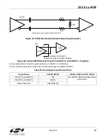
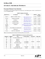
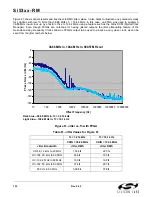
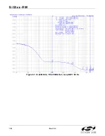
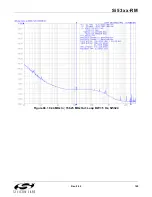
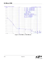
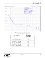
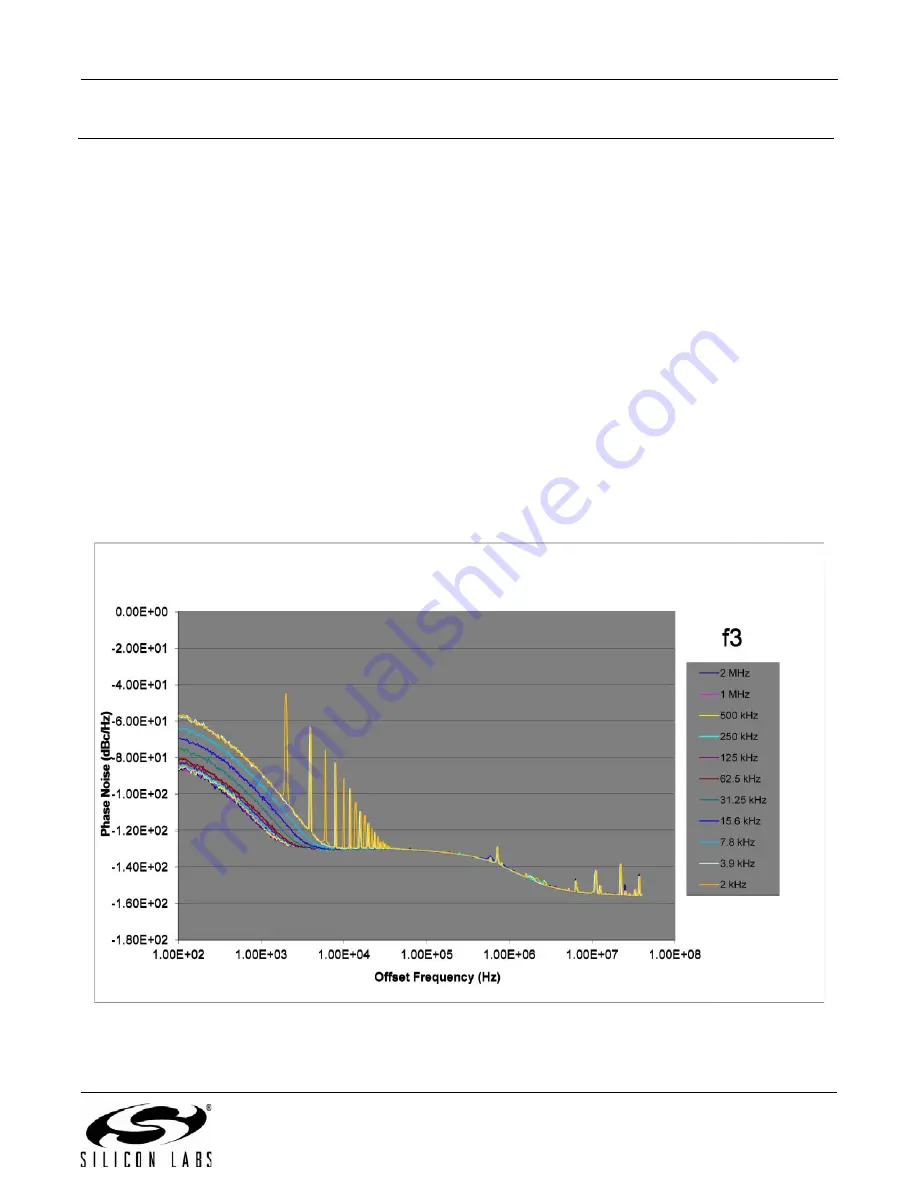
High f3 Value
f3 is defined as the comparison frequency at the Phase Detector. It is equal to the input frequency divided by N3.
DSPLL
sim
automatically picks the frequency plan that has the highest possible f3 value and it reports f3 for every
new frequency plan that it generates. f3 has a range from 2 kHz minimum up to 2 MHz maximum. The two main
causes of a low f3 are a low clock input frequency (which establishes an upper bound on f3) and a PLL multiplier
ratio that is comprised of large and mutually prime nominators and denominators. Specifically, for
CKOUT = CKIN x (P/Q), if P and Q are mutually prime and large in size, then f3 may have a low value. Very low
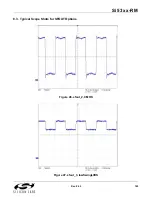
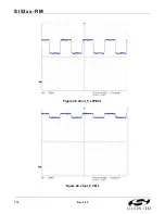
values of f3 usually result in extra jitter as can be seen in Figures 60 through 62 and in Table 61.
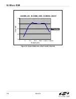
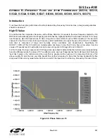
For the f3 study, the input, output and VCO frequencies were held constant while the dividers were manipulated by
hand to artificially reduce the value of f3. Two effects can be seen as f3 approaches the 2 kHz lower limit: there are
“spur like” spikes in the mid-band and the noise floor is elevated at the near end. It is also clear that once f3 is
above roughly 50 kHz, there is very little benefit from further increasing f3. Note that the loop bandwidth for this
study was 60 Hz and any noise below 60 Hz is a result of the input clock, not the Any-Frequency Precision Clock.
Figure 60. Phase Noise vs. f3
Summary of Contents for Si5316 Series
Page 2: ...Si53xx RM 2 Rev 0 52 ...
Page 110: ...Si53xx RM 110 Rev 0 52 Figure 48 sfout_5 LVPECL Figure 49 sfout_6 CML ...
Page 111: ...Si53xx RM Rev 0 52 111 Figure 50 sfout_7 LVDS ...
Page 127: ...Si53xx RM Rev 0 52 127 Figure 66 155 52 MHz In 622 08 MHz Out Loop BW 7 Hz Si5324 ...
Page 128: ...Si53xx RM 128 Rev 0 52 Figure 67 19 44 MHz In 156 25 MHz Out Loop BW 80 Hz ...
Page 129: ...Si53xx RM Rev 0 52 129 Figure 68 19 44 MHz In 156 25 MHz Out Loop BW 5 Hz Si5324 ...
Page 131: ...Si53xx RM Rev 0 52 131 Figure 70 61 44 MHz In 491 52 MHz Out Loop BW 7 Hz Si5324 ...
Page 132: ...Si53xx RM 132 Rev 0 52 Figure 71 622 08 MHz In 672 16 MHz Out Loop BW 6 9 kHz ...
Page 133: ...Si53xx RM Rev 0 52 133 Figure 72 622 08 MHz In 672 16 MHz Out Loop BW 100 Hz ...
Page 134: ...Si53xx RM 134 Rev 0 52 Figure 73 156 25 MHz In 155 52 MHz Out ...
Page 139: ...Si53xx RM Rev 0 52 139 Figure 78 86 685 MHz In 173 371 MHz Out ...
Page 140: ...Si53xx RM 140 Rev 0 52 Figure 79 86 685 MHz In 693 493 MHz Out ...
Page 142: ...Si53xx RM 142 Rev 0 52 Figure 81 10 MHz In 1 GHz Out ...
Page 174: ...Si53xx RM 174 Rev 0 52 Figure 99 Si5374 Si5375 DSPLL A ...
Page 175: ...Si53xx RM Rev 0 52 175 Figure 100 Si5374 Si5375 DSPLL B ...
Page 176: ...Si53xx RM 176 Rev 0 52 Figure 101 Si5374 Si5375 DSPLL C ...