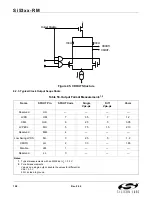


S i 5 3 x x - R M
122
Rev. 0.52
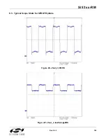
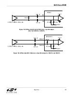
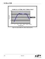
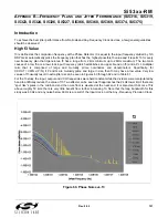
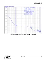
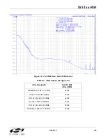
Figure 61
shows similar results and ties them to RMS jitter values. It also helps to illustrate one potential remedy
for solutions with low f3. Note that 38.88 MHz x 5 = 194.4 MHz. In this case, an FPGA was used to multiply a
38.88 MHz input clock up by a factor of five to 194.4 MHz, using a feature such as the Xilinx DCM (Digital Clock
Manager). Even though FPGAs are notorious for having jittered outputs, the jitter attenuating feature of the
Narrowband Any-Frequency Clocks allow an FPGA’s output to be used to produce a very clean clock, as can be
seen from the jitter numbers below.
Figure 61. Jitter vs. f3 with FPGA
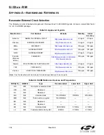
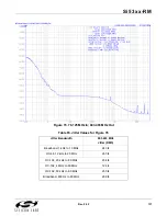
Table 61. Jitter Values for Figure 61
f3 = 3.214 kHz
f3 = 16.1 kHz
CKIN = 38.88 MHz
CKIN = 194.4 MHz
Jitter Bandwidth
Jitter, RMS
Jitter, RMS
OC-48, 12 kHz to 20 MHz
1,034 fs
285 fs
OC-192, 20 kHz to 80 MHz
668 fs
300 fs
OC-192, 4 MHz to 80 MHz
169 fs
168 fs
OC-192, 50 kHz to 80 MHz
374 fs
287 fs
800 Hz to 80 MHz
3,598 fs
378 fs
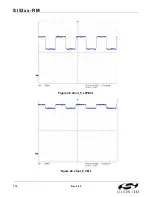
38.88 MHz in, 194.4 MHz in, 690.57 MHz out
-160
-140
-120
-100
-80
-60
-40
-20
0
10
100
1000
10000
100000
1000000
10000000 100000000
Offset Frequency (Hz)
P
h
ase N
o
is
e (
d
B
c/
H
z
)
Dark blue—38.88 MHz in, f3 = 3.214 kHz
Light blue—194.4 MHz in, f3 = 16.1 kHz
Summary of Contents for Si5316 Series
Page 2: ...Si53xx RM 2 Rev 0 52 ...
Page 110: ...Si53xx RM 110 Rev 0 52 Figure 48 sfout_5 LVPECL Figure 49 sfout_6 CML ...
Page 111: ...Si53xx RM Rev 0 52 111 Figure 50 sfout_7 LVDS ...
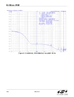
Page 127: ...Si53xx RM Rev 0 52 127 Figure 66 155 52 MHz In 622 08 MHz Out Loop BW 7 Hz Si5324 ...
Page 128: ...Si53xx RM 128 Rev 0 52 Figure 67 19 44 MHz In 156 25 MHz Out Loop BW 80 Hz ...
Page 129: ...Si53xx RM Rev 0 52 129 Figure 68 19 44 MHz In 156 25 MHz Out Loop BW 5 Hz Si5324 ...
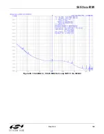
Page 131: ...Si53xx RM Rev 0 52 131 Figure 70 61 44 MHz In 491 52 MHz Out Loop BW 7 Hz Si5324 ...
Page 132: ...Si53xx RM 132 Rev 0 52 Figure 71 622 08 MHz In 672 16 MHz Out Loop BW 6 9 kHz ...
Page 133: ...Si53xx RM Rev 0 52 133 Figure 72 622 08 MHz In 672 16 MHz Out Loop BW 100 Hz ...
Page 134: ...Si53xx RM 134 Rev 0 52 Figure 73 156 25 MHz In 155 52 MHz Out ...
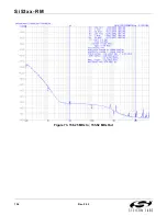
Page 139: ...Si53xx RM Rev 0 52 139 Figure 78 86 685 MHz In 173 371 MHz Out ...
Page 140: ...Si53xx RM 140 Rev 0 52 Figure 79 86 685 MHz In 693 493 MHz Out ...
Page 142: ...Si53xx RM 142 Rev 0 52 Figure 81 10 MHz In 1 GHz Out ...
Page 174: ...Si53xx RM 174 Rev 0 52 Figure 99 Si5374 Si5375 DSPLL A ...
Page 175: ...Si53xx RM Rev 0 52 175 Figure 100 Si5374 Si5375 DSPLL B ...
Page 176: ...Si53xx RM 176 Rev 0 52 Figure 101 Si5374 Si5375 DSPLL C ...